
What is 2.5D IC Package Substrate?
2.5D IC Package Substrate Manufacturing and 2.5D IC Package firm. High speed and high frequency material packaging substrate manufacturing. Advanced packaging substrate production process and Advanced 2.5D IC Package technology.
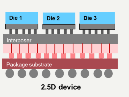
A 2.5D IC (Integrated Circuit) package substrate is a type of packaging technology used in semiconductor manufacturing. In a 2.5D IC package, multiple integrated circuits (ICs) or dies are stacked vertically on top of each other, with each die performing a specific function. These dies are interconnected using advanced packaging techniques, such as through-silicon vias (TSVs) or microbumps.
The “2.5D” terminology refers to the fact that the integration is not purely two-dimensional (2D), where components are placed side by side on a single plane, nor is it fully three-dimensional (3D), where multiple layers of transistors are vertically stacked within a single die. Instead, 2.5D IC packaging achieves a compromise between these two approaches by stacking separate dies on top of each other while still utilizing traditional packaging techniques for each individual die.
The package substrate in a 2.5D IC plays a critical role in providing electrical connections between the stacked dies, as well as heat dissipation and mechanical support. These substrates are typically made of advanced materials, such as organic substrates, silicon interposers, or glass interposers, depending on the specific requirements of the application.
Overall, 2.5D IC packaging enables higher levels of integration and performance compared to traditional 2D packaging, while offering some advantages over fully 3D stacked ICs, such as lower manufacturing complexity and cost. This technology is commonly used in applications such as high-performance computing, networking, and advanced consumer electronics.
What are the functions of 2.5D IC Package Substrate?
The functions of a 2.5D IC Package Substrate include, but are not limited to, the following:
Electrical connectivity: The substrate facilitates electrical connections between stacked chips by utilizing various interconnection technologies such as Through-Silicon Vias (TSVs) or microbumps.
Thermal dissipation: It helps in efficiently conducting and dissipating heat generated by the chips to ensure they operate within the appropriate temperature range, avoiding performance degradation or damage.
Mechanical support: The substrate provides mechanical support for the stacked chips to ensure stable connections between them and to provide necessary structural support during manufacturing, assembly, and usage.
Signal routing: Through layout, design, and control of signal transmission lines, the substrate aids in reducing signal transmission delay and distortion, enhancing data communication speed and reliability between chips.
Power distribution: The substrate can be designed to distribute power and ground lines to ensure stable power supply between stacked chips, ensuring their normal operation and performance.
In summary, the 2.5D IC Package Substrate plays a crucial role in integrated circuit stacking, providing not only physical connections but also impacting the performance, reliability, and cost-effectiveness of the entire packaging system.
What are the different types of 2.5D IC Package Substrate?
There are several types of 2.5D IC package substrates, each with its own characteristics and advantages. Some common types include:
Organic substrates: These substrates are made of organic materials such as epoxy resin or polyimide. They are cost-effective and offer good electrical properties, making them suitable for many applications. However, they may have limitations in terms of thermal conductivity and mechanical strength.
Silicon interposers: Silicon interposers are made of silicon wafers with embedded TSVs. They offer excellent electrical performance, high density interconnects, and good thermal conductivity. Silicon interposers are well-suited for high-performance applications but tend to be more expensive than organic substrates.
Glass interposers: Glass interposers utilize glass materials with embedded TSVs. They offer similar advantages to silicon interposers, such as high density interconnects and good thermal conductivity. Glass interposers may provide better cost-effectiveness compared to silicon interposers in some cases.
Ceramic substrates: Ceramic substrates, such as alumina or aluminum nitride, offer excellent thermal conductivity and mechanical strength. They are well-suited for high-power and high-temperature applications but tend to be more expensive than organic substrates.
Laminate substrates: Laminate substrates consist of multiple layers of organic or glass materials with embedded interconnects. They offer a balance between cost, performance, and flexibility, making them suitable for a wide range of applications.
These are just a few examples of the types of 2.5D IC package substrates available. The choice of substrate depends on factors such as performance requirements, cost considerations, and specific application needs.
What is the relationship between 2.5D IC Package Substrate and IC packaging?
The relationship between 2.5D IC package substrate and IC packaging is quite significant, as the substrate is a crucial component within the overall IC packaging process, especially in the context of 2.5D packaging technology.
IC packaging involves the assembly of individual semiconductor dies or chips into a package that provides electrical connections, protection, and sometimes thermal management for the integrated circuit. Traditionally, IC packaging has primarily been done in a two-dimensional (2D) manner, where chips are mounted side by side on a single substrate, such as a printed circuit board (PCB).
In contrast, 2.5D IC packaging introduces the concept of vertical stacking, where multiple chips are stacked on top of each other, connected through advanced packaging techniques like through-silicon vias (TSVs) or microbumps. The package substrate plays a critical role in facilitating these vertical connections between the stacked chips.
The substrate in a 2.5D IC package provides several functions essential to the overall packaging process, including:
Electrical connectivity: The substrate enables electrical connections between the stacked chips, allowing for signal transmission and power distribution.
Thermal management: It helps dissipate heat generated by the stacked chips, ensuring they operate within acceptable temperature ranges to maintain performance and reliability.
Mechanical support: The substrate provides structural support for the stacked chips, ensuring their stability and integrity during manufacturing, handling, and operation.
Signal routing and integrity: The substrate facilitates the routing of signals between the stacked chips while maintaining signal integrity to minimize signal degradation and interference.
Overall, the 2.5D IC package substrate is an integral part of the IC packaging process, particularly in enabling the vertical integration of multiple chips and ensuring the performance, reliability, and functionality of the packaged semiconductor device.
2.5D IC Package Substrate
How does 2.5D IC Package Substrate differ from PCB?
2.5D IC package substrate and PCB (Printed Circuit Board) are both critical components in electronic systems, but they serve different purposes and exhibit several key differences:
Functionality:
2.5D IC package substrate: Its primary function is to provide electrical connections and mechanical support for the vertical stacking of multiple semiconductor chips (ICs) within a package. It facilitates the integration of multiple chips, often with different functions, into a single package.
PCB: PCBs serve as platforms for mounting and interconnecting various electronic components such as ICs, resistors, capacitors, and connectors in a two-dimensional layout. They provide electrical connections between components and mechanical support for the entire electronic system.
Complexity of Interconnects:
2.5D IC package substrate: These substrates typically involve advanced interconnection technologies such as through-silicon vias (TSVs) or microbumps to enable vertical stacking of chips and high-density interconnects between them.
PCB: PCBs usually utilize simpler interconnection methods such as copper traces, vias, and solder joints for surface-mount components. They are primarily designed for planar interconnections.
Material and Manufacturing:
2.5D IC package substrate: These substrates often use specialized materials such as silicon interposers, glass interposers, or organic substrates with embedded TSVs. Manufacturing processes involve advanced semiconductor fabrication techniques.
PCB: PCBs are typically made from fiberglass-reinforced epoxy laminate with copper traces and vias. Their manufacturing involves processes like etching, drilling, and soldering, which are different from semiconductor fabrication processes.
Application and Integration:
2.5D IC package substrate: These substrates are commonly used in high-performance computing, networking, and advanced consumer electronics where high integration density and performance are required.
PCB: PCBs are ubiquitous in various electronic devices, from simple consumer electronics to complex industrial systems. They provide the foundation for the integration of electronic components in these systems.
In summary, while both 2.5D IC package substrates and PCBs play essential roles in electronic systems, they differ in functionality, complexity of interconnects, materials, manufacturing processes, and applications. The 2.5D IC package substrate is specifically designed for enabling the vertical integration of semiconductor chips, while PCBs are more versatile and widely used for interconnecting electronic components in two-dimensional layouts.
What are the structure and production technology of 2.5D IC Package Substrate?
The structure and production technology of a 2.5D IC package substrate can vary depending on the specific materials and manufacturing processes used. However, here is a generalized overview of the typical structure and production technology:
Structure:
Base Material: The substrate usually starts with a base material, which can be organic (such as epoxy resin or polyimide), inorganic (such as silicon or glass), or a combination of both.
Interconnection Layer: This layer contains the wiring patterns and vias that provide electrical connections between the stacked semiconductor chips. Advanced interconnection technologies like through-silicon vias (TSVs) or microbumps may be utilized for vertical stacking.
Dielectric Layer: Dielectric materials are often used to insulate and separate the wiring layers, preventing electrical shorts and interference.
Passivation Layer: A passivation layer is applied to protect the wiring and interconnections from environmental factors such as moisture, contamination, and mechanical stress.
Surface Finish: The substrate’s surface may be finished with materials like solder mask or metal layers for soldering components and providing additional electrical connections.
Production Technology:
Substrate Fabrication: The production process typically starts with the fabrication of the base material, which may involve processes like casting, molding, or deposition, depending on the material used.
Interconnection Formation: Advanced lithography and etching techniques are used to create intricate wiring patterns and vias on the substrate surface. For TSVs, drilling and filling techniques are employed to create vertical connections between layers.
Dielectric Deposition and Planarization: Dielectric materials are deposited onto the substrate surface and planarized to create smooth, uniform layers between the wiring layers.
Passivation and Surface Finishing: A passivation layer is applied to protect the substrate’s surface, followed by the application of surface finishes like solder mask or metal layers using techniques such as coating, printing, or plating.
Chip Attachment and Packaging: Once the substrate is prepared, semiconductor chips are attached and interconnected using techniques like flip-chip bonding, wire bonding, or soldering. The assembled package may undergo further processes such as encapsulation, testing, and inspection before being integrated into electronic systems.
Overall, the production of 2.5D IC package substrates involves a combination of semiconductor fabrication techniques, materials science, and traditional PCB manufacturing processes to create complex structures capable of enabling high-density integration and vertical stacking of semiconductor chips.
Frequently Asked Questions (FAQs)
What is a 2.5D IC Package Substrate?
A 2.5D IC Package Substrate is a critical component in semiconductor packaging technology, facilitating the vertical stacking of multiple semiconductor chips (ICs) in a single package. It provides electrical connections, thermal management, and mechanical support for the stacked chips.
How does a 2.5D IC Package Substrate differ from a PCB?
While both serve as platforms for interconnecting electronic components, a 2.5D IC Package Substrate is specifically designed for enabling vertical chip stacking, whereas a PCB primarily facilitates two-dimensional interconnections.
What are the common types of 2.5D IC Package Substrates?
Common types include organic substrates, silicon interposers, glass interposers, ceramic substrates, and laminate substrates. Each type offers different characteristics and advantages based on the application requirements.
What are the key functions of a 2.5D IC Package Substrate?
The functions include providing electrical connectivity between stacked chips, dissipating heat generated by the chips, offering mechanical support, routing signals between chips, and distributing power within the package.
What are the production technologies involved in manufacturing 2.5D IC Package Substrates?
Production technologies include substrate fabrication, interconnection formation using advanced lithography and etching techniques, dielectric deposition and planarization, passivation, surface finishing, chip attachment, and packaging processes.
What are the applications of 2.5D IC Package Substrates?
2.5D IC Package Substrates are commonly used in high-performance computing, networking, advanced consumer electronics, and other applications requiring high integration density and performance.
What are the advantages of using 2.5D IC Package Substrates?
Advantages include increased integration density, improved performance, reduced form factor, enhanced thermal management, and potential cost savings compared to traditional packaging technologies.
What challenges are associated with the adoption of 2.5D IC Package Substrates?
Challenges include high manufacturing complexity, development of advanced interconnection technologies, thermal management issues, and cost considerations.
Conclusion
In conclusion, 2.5D IC Package Substrates represent an advanced packaging technology that enables the vertical stacking of multiple semiconductor chips within a single package. These substrates play a crucial role in facilitating high-density integration, improved performance, and enhanced thermal management in electronic systems. By providing electrical connections, dissipating heat, offering mechanical support, and routing signals between stacked chips, 2.5D IC Package Substrates contribute to the development of innovative solutions in high-performance computing, networking, and advanced consumer electronics.
While 2.5D IC Package Substrates offer numerous advantages such as increased integration density and improved performance, they also present challenges such as high manufacturing complexity and thermal management issues. However, ongoing advancements in materials science, manufacturing processes, and interconnection technologies continue to address these challenges and drive the adoption of 2.5D IC Package Substrates in various applications.
Overall, 2.5D IC Package Substrates represent a significant evolution in semiconductor packaging technology, offering opportunities for improved functionality, efficiency, and cost-effectiveness in electronic systems. As the demand for higher performance and miniaturization continues to grow, the role of 2.5D IC Package Substrates is expected to become even more prominent in shaping the future of electronics.