
What is 3D IC Package Substrate?
3D IC Package Substrate Provider and 3D IC Package Service.High speed and high frequency material packaging substrate manufacturing. Advanced packaging substrate production process and Package technology.
A 3D IC package substrate refers to the substrate used in the construction of three-dimensional integrated circuit (3D IC) packages. In traditional IC packaging, integrated circuits are typically mounted on a two-dimensional substrate, such as a printed circuit board (PCB). However, with the advancement of technology and the need for more compact and efficient designs, 3D IC packaging has emerged as a solution.
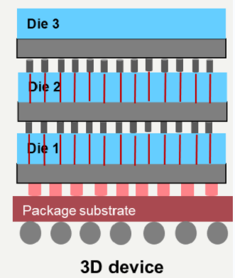
In 3D IC packaging, multiple layers of integrated circuits are stacked vertically on top of each other, connected by through-silicon vias (TSVs) or other interconnect technologies. The 3D IC package substrate serves as a base for these stacked layers, providing structural support and electrical connectivity between the integrated circuits.
The substrate used in 3D IC packaging must meet various requirements, including high electrical conductivity, thermal conductivity for efficient heat dissipation, mechanical strength to support the stacked layers, and compatibility with advanced packaging processes such as TSV fabrication. Materials commonly used for 3D IC package substrates include silicon, glass, and various types of organic and inorganic materials.
Overall, the 3D IC package substrate plays a crucial role in enabling the construction of compact, high-performance integrated circuits with enhanced functionality and efficiency.
3D IC Package Substrate
What are the functions of 3D IC Package Substrate?
The functions of a 3D IC package substrate include:
Structural support: The substrate provides the structural framework to support the stacked layers of integrated circuits, ensuring the stability and reliability of the entire packaging structure.
Electrical connectivity: Through conductive pathways, the package substrate connects the integrated circuits in different layers, enabling them to communicate and exchange data.
Thermal management: By designing effective thermal dissipation pathways within the substrate, 3D IC package substrates help efficiently conduct and dissipate the heat generated by the integrated circuits, ensuring temperature stability and performance.
Signal transmission: The package substrate provides pathways for signal transmission, ensuring reliable data transfer and communication between integrated circuits in different layers.
Packaging encapsulation: The substrate can provide external protection for the package, ensuring that the integrated circuits are protected from environmental factors such as moisture, dust, etc.
In summary, 3D IC package substrates play a crucial role in the stacked packaging of multi-layer integrated circuits, providing structural support, electrical connectivity, thermal management, and ensuring stability, performance, and reliability of the packaging.
What are the different types of 3D IC Package Substrate?
There are several types of 3D IC package substrates, each with its own characteristics and advantages. Some of the commonly used types include:
Silicon Interposer: A silicon interposer is a silicon wafer with through-silicon vias (TSVs) that provide vertical connections between stacked integrated circuits. Silicon interposers offer high electrical performance, low signal loss, and compatibility with standard semiconductor manufacturing processes.
Glass Interposer: Glass interposers utilize glass substrates with TSVs to facilitate vertical integration of stacked ICs. Glass interposers offer advantages such as high thermal conductivity, excellent electrical properties, and low signal loss. They are also lightweight and have good optical transparency.
Organic Interposer: Organic interposers use organic substrates, such as laminates or build-up films, with embedded TSVs for vertical connectivity. Organic interposers are lightweight, cost-effective, and offer good electrical performance. However, they may have limitations in terms of thermal conductivity compared to silicon or glass interposers.
Silicon Substrate: In some cases, the 3D IC package substrate may be made entirely of silicon, with TSVs formed directly in the silicon substrate. Silicon substrates offer excellent electrical and thermal properties, making them suitable for high-performance applications. However, they may be more expensive and challenging to manufacture compared to other substrate types.
Ceramic Substrate: Ceramic substrates, such as alumina or aluminum nitride, can also be used for 3D IC packaging. Ceramic substrates offer high thermal conductivity, excellent mechanical properties, and good electrical insulation. They are suitable for applications requiring high reliability and thermal performance.
Flex Substrate: Flexible substrates, such as flexible printed circuit boards (PCBs), can be used for 3D IC packaging in applications requiring flexibility or conformability. Flex substrates offer advantages such as lightweight, compactness, and the ability to bend or conform to non-planar surfaces.
These are some of the common types of 3D IC package substrates used in various applications, each offering different characteristics and benefits depending on the specific requirements of the application.
What is the relationship between 3D IC Package Substrate and IC packaging?
The relationship between 3D IC package substrate and IC packaging is integral and symbiotic. IC packaging refers to the process of enclosing integrated circuits (ICs) in protective cases and providing electrical connections to external circuitry. The substrate serves as the foundation upon which ICs are mounted and interconnected within the package. In the context of 3D IC packaging, the substrate plays an even more critical role as it facilitates the stacking of multiple IC layers.
Here’s how the relationship between 3D IC package substrate and IC packaging works:
Structural Support: The substrate provides structural support for the stacked IC layers in 3D IC packaging. It ensures the stability and integrity of the package by holding the ICs in place and distributing mechanical stresses.
Electrical Connectivity: The substrate facilitates electrical connections between ICs within the package and external circuitry. Through the use of conductive traces and vias, the substrate enables signal transmission and power distribution between different IC layers and external components.
Thermal Management: Effective thermal management is crucial in IC packaging to dissipate heat generated by the ICs and maintain optimal operating temperatures. The substrate plays a significant role in heat dissipation by providing thermal pathways and interfaces for heat transfer to external heat sinks or thermal solutions.
Integration with Packaging Technologies: The choice of substrate material and design is closely linked to the packaging technologies employed in 3D IC packaging. Substrates must be compatible with advanced packaging techniques such as through-silicon vias (TSVs), flip-chip bonding, and wafer-level packaging to enable efficient stacking and interconnection of IC layers.
Packaging Encapsulation: In addition to providing electrical and mechanical support, the substrate may also contribute to the encapsulation and protection of the ICs within the package. This encapsulation shields the ICs from environmental factors such as moisture, dust, and mechanical shocks, enhancing their reliability and longevity.
In summary, the 3D IC package substrate is an essential component of IC packaging, particularly in 3D IC packaging where multiple IC layers are stacked vertically. It provides structural support, electrical connectivity, thermal management, and packaging encapsulation, enabling the integration and functionality of complex semiconductor devices.
How does 3D IC Package Substrate differ from PCB?
While both 3D IC package substrates and printed circuit boards (PCBs) serve as platforms for mounting and interconnecting electronic components, they differ significantly in terms of their design, materials, and applications. Here are some key differences between 3D IC package substrates and PCBs:
Purpose and Functionality:
3D IC Package Substrate: The primary purpose of a 3D IC package substrate is to provide structural support, electrical connectivity, and thermal management for vertically stacked integrated circuits (ICs) in 3D IC packaging. It enables the integration of multiple IC layers within a single package, allowing for increased functionality and performance.
PCB: PCBs are used for mounting and interconnecting electronic components in two-dimensional configurations. They provide a platform for attaching ICs, resistors, capacitors, and other electronic components, enabling the assembly of complex electronic systems such as computers, smartphones, and automotive electronics.
Design and Complexity:
3D IC Package Substrate: The design of a 3D IC package substrate is optimized for vertical integration and stacking of IC layers. It may incorporate features such as through-silicon vias (TSVs), microbumps, and redistribution layers (RDLs) to facilitate electrical connections between stacked ICs and external circuitry. The design complexity is higher compared to PCBs due to the need for advanced packaging techniques and technologies.
PCB: PCBs typically consist of multiple layers of copper traces and insulating substrates (e.g., fiberglass or epoxy resin). They may feature complex routing patterns and components arranged in a planar layout. While PCBs can be designed with high complexity, they do not involve the vertical integration of IC layers as seen in 3D IC package substrates.
Materials:
3D IC Package Substrate: 3D IC package substrates are often made of semiconductor materials such as silicon or glass, as well as organic substrates with embedded TSVs. These materials offer high electrical conductivity, thermal conductivity, and compatibility with advanced packaging processes.
PCB: PCBs are typically constructed using fiberglass or epoxy resin laminates with copper layers. Other materials, such as ceramic or flexible substrates, may also be used for specific applications. PCB materials are chosen based on factors such as electrical performance, mechanical strength, and cost.
Applications:
3D IC Package Substrate: 3D IC package substrates are primarily used in advanced semiconductor packaging applications, such as high-performance computing, mobile devices, and automotive electronics, where compactness, performance, and integration are critical.
PCB: PCBs are used in a wide range of electronic devices and systems, including consumer electronics, industrial equipment, medical devices, and telecommunications infrastructure. They are suitable for applications that require cost-effective and reliable interconnection of electronic components.
In summary, while both 3D IC package substrates and PCBs play essential roles in electronic systems, they differ in their design, materials, and applications. 3D IC package substrates are specialized for vertically stacked IC integration, whereas PCBs are used for two-dimensional mounting and interconnection of electronic components.
What are the structure and production technology of 3D IC Package Substrate?
The structure and production technology of 3D IC package substrates can vary depending on the specific design requirements and materials used. However, here is a general overview of the typical structure and production processes involved in manufacturing 3D IC package substrates:
Structure:
Base Material: The substrate material serves as the foundation for the 3D IC package. Common substrate materials include silicon, glass, organic substrates (e.g., laminates or build-up films), ceramic, and flexible materials (e.g., flexible PCBs).
Through-Silicon Vias (TSVs): TSVs are vertical electrical connections that penetrate through the substrate material, enabling communication between different layers of integrated circuits (ICs). TSVs are typically filled with conductive material (e.g., copper) to provide electrical conductivity.
Redistribution Layers (RDLs): RDLs are metal layers patterned on the substrate surface to redistribute electrical signals between ICs and external circuitry. RDLs are essential for routing signals from TSVs to the appropriate locations on the substrate.
Dielectric Layers: Dielectric layers are insulating materials deposited between metal layers to provide electrical isolation and prevent signal interference.
Surface Finishes: Surface finishes such as solder mask and metal pads are applied to the substrate surface to protect the circuitry and facilitate soldering of ICs and other components.
Production Technology:
Substrate Fabrication: The production process begins with the fabrication of the substrate material. Depending on the material used (e.g., silicon wafer, glass panel, or flexible film), various manufacturing techniques such as semiconductor processing, glass molding, or roll-to-roll manufacturing may be employed.
TSV Fabrication: TSVs are typically formed using semiconductor processing techniques such as deep reactive ion etching (DRIE) or laser drilling. After the vias are created, they are filled with conductive material (e.g., copper) using techniques like electroplating or chemical vapor deposition (CVD).
RDL Formation: Redistribution layers are patterned on the substrate surface using photolithography, thin-film deposition (e.g., sputtering or evaporation), and etching processes. Multiple metal layers may be deposited and patterned to create complex routing patterns.
Dielectric Deposition: Insulating dielectric layers are deposited between metal layers using techniques such as chemical vapor deposition (CVD) or spin coating. These dielectric layers provide electrical isolation and mechanical support.
Surface Finishing: Once the circuitry is fabricated, surface finishes such as solder mask and metal pads are applied to the substrate surface using techniques like screen printing or photolithography.
Overall, the production of 3D IC package substrates involves a combination of semiconductor processing, thin-film deposition, photolithography, and other advanced manufacturing techniques to create complex structures with high-density interconnects and electrical functionality.
Frequently Asked Questions (FAQs):
What is a 3D IC package substrate?
A 3D IC package substrate is a specialized substrate used in three-dimensional integrated circuit (3D IC) packaging. It provides structural support, electrical connectivity, and thermal management for vertically stacked integrated circuits.
How does a 3D IC package substrate differ from a printed circuit board (PCB)?
While both serve as platforms for mounting and interconnecting electronic components, 3D IC package substrates are optimized for vertical integration and stacking of IC layers, whereas PCBs are used for two-dimensional configurations. 3D IC package substrates also incorporate advanced features such as through-silicon vias (TSVs) and redistribution layers (RDLs) for interconnection.
What are the different types of 3D IC package substrates?
Common types include silicon interposers, glass interposers, organic interposers, silicon substrates, ceramic substrates, and flexible substrates. Each type offers different characteristics and advantages depending on the specific application requirements.
What is the production technology involved in manufacturing 3D IC package substrates?
The production process typically involves substrate fabrication, TSV fabrication, redistribution layer formation, dielectric deposition, and surface finishing. Various semiconductor processing, thin-film deposition, photolithography, and other advanced manufacturing techniques are used to create complex structures with high-density interconnects.
What are the applications of 3D IC package substrates?
3D IC package substrates are used in advanced semiconductor packaging applications such as high-performance computing, mobile devices, automotive electronics, and data centers. They enable compact, high-density integration of multiple IC layers, resulting in improved performance, power efficiency, and miniaturization.
Conclusion
In conclusion, 3D IC package substrates play a vital role in advanced semiconductor packaging by enabling the vertical integration and stacking of multiple layers of integrated circuits (ICs). These substrates provide structural support, electrical connectivity, thermal management, and packaging encapsulation for the stacked ICs, contributing to improved performance, power efficiency, and miniaturization in electronic devices and systems.
Various types of 3D IC package substrates, including silicon interposers, glass interposers, organic interposers, silicon substrates, ceramic substrates, and flexible substrates, offer different characteristics and advantages to meet the diverse requirements of different applications.
The production technology involved in manufacturing 3D IC package substrates includes substrate fabrication, TSV fabrication, redistribution layer formation, dielectric deposition, and surface finishing. Advanced semiconductor processing, thin-film deposition, photolithography, and other manufacturing techniques are employed to create complex structures with high-density interconnects.
Overall, 3D IC package substrates represent a key enabling technology for the continued advancement of semiconductor packaging, driving innovation in areas such as high-performance computing, mobile devices, automotive electronics, and data centers. Their importance is expected to grow as demand for compact, high-performance electronic systems continues to increase.