
What is ABF Substrate
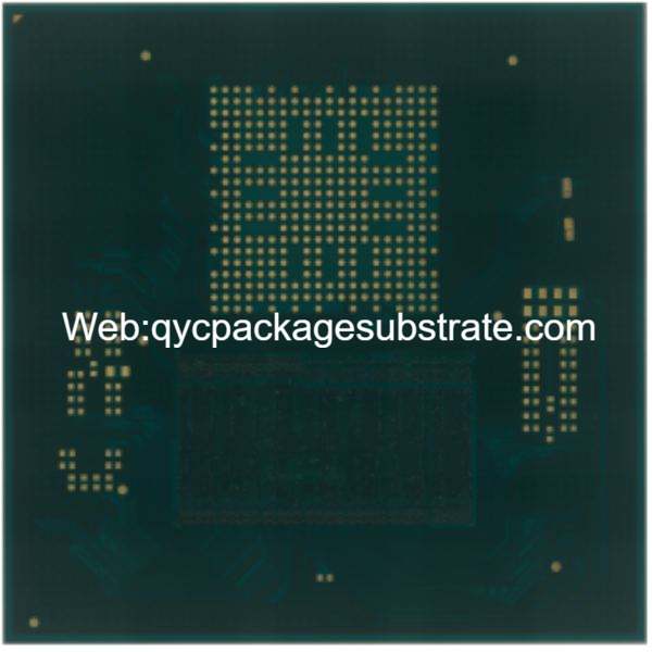
ABF Substrate Supplier. the FC BGA substrates were made with Showa Denko and ABF Ajinomoto materials. microtrace and spacing. we can use the ABF base to make 20 layers BGA substrates with high quality and fast lead time.
ABF Substrate, short for Amorphous Binary Fluoride Substrate, refers to a type of substrate material used in the construction of electronic devices and integrated circuits. It is characterized by its unique composition, containing amorphous binary fluoride, and offers exceptional electrical properties and thermal stability.
In this context, the term “substrate” pertains to the foundational material or base on which electronic components, like semiconductor chips, are constructed. Due to its distinct composition, ABF Substrate plays a pivotal role in offering essential support to these components, thereby enhancing the overall performance and reliability of electronic devices.
Key features of ABF Substrate include high thermal conductivity and low dielectric loss, making it particularly well-suited for applications requiring efficient heat dissipation and minimal electrical signal loss. As electronic devices become more advanced and compact, the properties of the substrate material play a critical role in ensuring optimal functionality and longevity.
ABF Substrate finds applications in various high-performance electronic devices, including those used in telecommunications, computing, and other industries where reliability and efficiency are paramount. Its use is often associated with advanced packaging solutions, contributing to the continued evolution of integrated circuit technology.
How Does ABF Substrate Contribute to Electronic Devices?
Anisotropic Conductive Film (ACF) or Anisotropic Conductive Adhesive (ACA) is a specialized adhesive film incorporating conductive particles. Its frequent application in electronic devices involves establishing electrical connections between surfaces, such as linking a flexible printed circuit (FPC) to a display or other electronic components.
Here’s how ABF substrate contributes to electronic devices, focusing on its mechanical support, electrical functionality, and thermal role:
Mechanical Support:
Flexibility: ABF substrates are typically flexible, making them suitable for applications where traditional rigid substrates are impractical. This flexibility allows for the integration of electronic components in devices with complex form factors or those that require bending and folding.
Thin Profile: ABF substrates are thin, contributing to the overall slim profile of electronic devices. This is especially important in applications like smartphones, wearables, and other portable electronics where space is at a premium.
Electrical Functionality:
Conductivity: The primary function of ABF substrate is to provide electrical connectivity between various components in electronic devices. The conductive particles within the substrate form paths that allow for the transmission of electrical signals. This is crucial for ensuring proper functioning of the device.
Anisotropic Conductivity: ABF substrates exhibit anisotropic conductivity, meaning that they conduct electricity in one direction only. This property allows for precise routing of electrical signals, preventing cross-talk and interference between adjacent conductive paths.
Thermal Role:
Heat Dissipation: In electronic devices, particularly those boasting high processing power, effectively managing heat is of paramount importance. ABF substrates, owing to their slender profile and direct interface with electronic components, play a pivotal role in dissipating the heat generated during operational processes.
Thermal Management: ABF substrates can play a role in the overall thermal management strategy of electronic devices. By efficiently conducting heat away from sensitive components, they help maintain optimal operating temperatures, preventing overheating and potential damage.
Ideal Solution for Advanced Packaging:
Miniaturization: ABF substrates support the trend of miniaturization in electronic devices by offering a compact and lightweight solution for interconnecting components.
Advanced Integration: The flexibility and thin profile of ABF substrates enable advanced packaging techniques, such as 3D stacking of components, which can lead to improved performance and functionality in compact form factors.
Reliability: ABF substrates are designed to provide reliable electrical connections over time, ensuring the long-term functionality and durability of electronic devices.
In summary, ABF substrate contributes significantly to electronic devices by providing mechanical support, facilitating electrical functionality, and playing a role in thermal management. Its unique properties make it an ideal solution for advanced packaging, enabling the development of compact, flexible, and high-performance electronic devices.
What Are the Different Types of ABF Substrate?
Various types of Anisotropic Conductive Film (ACF) or Anisotropic Conductive Adhesive (ACA) substrates exist, each characterized by unique structures and performance attributes. This diversity within ABF substrates caters to various electronic applications. Here, we’ll explore some common types:
Standard ABF Substrate:
Structure: Standard ABF substrates typically consist of a flexible film with conductive particles dispersed throughout.
Performance: They offer basic electrical connectivity and flexibility, suitable for applications where standard interconnectivity is sufficient.
High-Density ABF Substrate:
Structure: High-density ABF substrates are designed with a more refined structure, often featuring a higher concentration of conductive particles.
Performance: These substrates are ideal for applications requiring a higher density of electrical connections, enabling more intricate circuit designs.
Ultra-Thin ABF Substrate:
Structure: Ultra-thin ABF substrates focus on minimizing thickness while maintaining electrical conductivity.
Performance: These substrates contribute to the slim profiles of electronic devices, supporting the trend of creating thinner and more compact products.
Thermally Conductive ABF Substrate:
Structure: Thermally conductive ABF substrates incorporate materials with enhanced thermal conductivity.
Performance: They are designed to not only provide electrical connectivity but also contribute significantly to heat dissipation, making them suitable for applications with increased thermal management requirements.
High-Temperature Resistant ABF Substrate:
Structure: High-temperature resistant ABF substrates utilize materials capable of withstanding elevated temperatures.
Performance: These substrates are suitable for electronic devices that operate in environments with higher temperature ranges, ensuring long-term reliability.
Flexible ABF Substrate:
Structure: Flexible ABF substrates are engineered to offer exceptional flexibility, allowing them to conform to curved or irregular surfaces.
Performance: They are crucial for applications where the substrate needs to bend or flex, such as in wearable devices or flexible electronics.
Double-Sided ABF Substrate:
Structure: Double-sided ABF substrates feature conductive particles on both sides of the film.
Performance: This type facilitates the creation of complex interconnections and is useful in applications where components on both sides of the substrate require electrical connectivity.
Understanding the different types of ABF substrates enables engineers and designers to choose the most suitable variant for specific electronic applications, considering factors such as electrical requirements, flexibility, thermal management, and space constraints.
How Does ABF Substrate Relate to Integrated Circuit Packaging?
ABF substrate plays a crucial role in integrated circuit (IC) packaging, contributing significantly to the overall performance and reliability of highly integrated electronic devices. Here’s an exploration of the relationship between ABF substrate and integrated circuit packaging, highlighting its categorization in chip packaging technology:
Categorization in Chip Packaging Technology:
Flip Chip Technology: ABF substrate is frequently utilized in flip chip packaging, a technology where the IC is directly mounted face-down onto the substrate. The conductive particles in the ABF substrate establish electrical connections between the IC and the substrate, allowing for efficient signal transmission.
Wafer-Level Packaging (WLP): In WLP, ABF substrates are used to create the package at the wafer level before individual ICs are singulated. This approach enhances manufacturing efficiency and is well-suited for miniaturized and high-density applications.
System-in-Package (SiP): ABF substrates find application in SiP, a packaging technique that integrates multiple ICs and other components into a single package. The substrate facilitates interconnections between the various elements, promoting compactness and improved overall performance.
Pivotal Role in Highly Integrated Electronic Devices:
Miniaturization: ABF substrates contribute to the trend of miniaturization in electronic devices by enabling compact and space-efficient packaging. This is essential for devices such as smartphones, wearables, and IoT devices where size constraints are critical.
High-Density Interconnections: The conductive nature of ABF substrates allows for high-density interconnections between the IC and other components. This is crucial for achieving the intricate circuit designs required for advanced electronic devices.
Flexible Electronics: ABF substrates, being flexible, are well-suited for applications in flexible and bendable electronics. This flexibility is particularly valuable in devices like foldable displays and wearable technology.
Improved Thermal Management: The thin profile of ABF substrates facilitates efficient heat dissipation from the IC, contributing to better thermal management. This is essential in devices with high processing power where heat dissipation is a critical consideration.
Reliability: ABF substrates are designed for reliable and durable performance. Their use in integrated circuit packaging ensures stable electrical connections over time, contributing to the overall reliability of electronic devices.
In summary, the relationship between ABF substrate and integrated circuit packaging is integral to the advancement of chip packaging technology. ABF substrates support various packaging methods, play a pivotal role in achieving miniaturization and high-density interconnections, and contribute to the overall reliability and performance of highly integrated electronic devices.
What Sets ABF Substrate Apart from Traditional PCBs?
ABF substrate differs significantly from traditional Printed Circuit Boards (PCBs), encompassing distinctive features in terms of materials, construction, and applications. Here’s a comparison, emphasizing differences in motherboards, substrates, Substrate-Like PCBs (SLP), and High-Density Interconnect (HDI) boards:
Material Composition:
ABF Substrate: Anisotropic Conductive Film (ACF) or Anisotropic Conductive Adhesive (ACA) substrates are typically composed of a flexible film with dispersed conductive particles. These films are designed to provide electrical connectivity in a thin and flexible format.
Traditional PCBs: Traditional PCBs, on the other hand, are commonly made of rigid materials such as fiberglass reinforced with epoxy (FR-4). The rigidity of these boards makes them suitable for many standard applications.
Flexibility:
ABF Substrate: ABF substrates are inherently flexible, allowing them to conform to irregular shapes and making them ideal for applications where flexibility is crucial, such as in wearable devices or flexible electronics.
Traditional PCBs: Traditional PCBs are typically rigid, limiting their use in applications where flexibility is a key requirement.
Motherboard Applications:
ABF Substrate: ABF substrates are often used in the packaging of integrated circuits, contributing to the miniaturization and enhanced performance of electronic devices. They are commonly employed in chip packaging technologies, such as flip-chip and wafer-level packaging.
Traditional PCBs: Traditional PCBs are commonly found in motherboards and other applications where a rigid platform is needed to support various components.
Substrate-Like PCBs (SLP):
ABF Substrate: ABF substrates share similarities with Substrate-Like PCBs (SLP) in terms of flexibility and thin profile. Both are designed to offer a more compact and lightweight solution compared to traditional rigid PCBs.
Traditional PCBs: Traditional PCBs, being rigid, differ significantly from both ABF substrates and SLP in terms of form factor and application.
High-Density Interconnect (HDI) Boards:
ABF Substrate: ABF substrates often contribute to achieving high-density interconnections, especially in advanced packaging technologies. The conductive particles within the substrate enable precise routing of electrical signals in a compact space.
Traditional PCBs: While HDI boards also aim for high-density interconnections, they achieve this through advanced PCB manufacturing techniques, such as microvias and fine-line traces, rather than the use of flexible film with conductive particles.
In summary, ABF substrate stands apart from traditional PCBs due to its flexibility, use in chip packaging technologies, and its role in achieving high-density interconnections. While traditional PCBs remain essential for many applications, ABF substrates provide a unique solution for miniaturized, flexible, and highly integrated electronic devices.
What Constitutes the Structure and Production Technologies of ABF Substrate?
The configuration of Anisotropic Conductive Film (ACF) or Anisotropic Conductive Adhesive (ACA) substrates is crucial for their electronic device performance. The manufacturing technologies utilized in their production have advanced, integrating sophisticated methods like High-Density Interconnect (HDI) fabrication and inventive semi-additive processes.Here’s an exploration of the main structure of ABF substrate and the production technologies associated with it:
Structure of ABF Substrate:
Flexible Film Base: The foundation of ABF substrate is a flexible film, typically made of materials like polyimide. This flexible base allows the substrate to conform to various shapes and provides versatility in applications requiring flexibility.
Conductive Particles: Dispersed within the flexible film are conductive particles, which are crucial for establishing electrical connections. These particles are anisotropic, meaning they conduct electricity in one direction only, allowing for precise routing of electrical signals.
Adhesive Layer: ABF substrates often include an adhesive layer that helps bond the substrate to other components, such as integrated circuits or display panels. This layer enhances the mechanical stability of the overall assembly.
Production Technologies:
HDI Fabrication Technology: HDI fabrication technology is employed to achieve high-density interconnects in ABF substrates. This involves advanced PCB manufacturing techniques such as microvias, fine-line traces, and multiple layers. HDI technology allows for a more compact design with increased routing density.
Semi-Additive Method: The semi-additive method is an innovative approach to the production of ABF substrates. In this method, only the necessary conductive traces are added to the substrate, minimizing material usage and enhancing precision. This process is particularly advantageous in achieving high-density interconnects with improved signal integrity.
Roll-to-Roll Manufacturing: Some ABF substrates are produced using roll-to-roll manufacturing processes. This continuous manufacturing method involves feeding a flexible substrate through a series of processes, allowing for efficient and scalable production. Roll-to-roll manufacturing is well-suited for applications requiring large volumes of flexible and thin substrates.
Precision Printing: Precision printing technologies, such as screen printing or inkjet printing, may be employed to deposit conductive materials onto the flexible film. This allows for the creation of intricate conductive patterns with high precision.
Lamination Techniques: Lamination is a critical step in ABF substrate production, where multiple layers are bonded together. This process ensures the integrity of the substrate and helps in achieving the desired mechanical and electrical properties.
These production technologies collectively contribute to the creation of ABF substrates with specific characteristics, including flexibility, thin profile, and high-density interconnectivity. The advancements in HDI fabrication, semi-additive methods, and roll-to-roll manufacturing have played a key role in enhancing the performance and efficiency of ABF substrates in various electronic applications.
What are Frequently Asked Questions (FAQs) about ABF Substrate?
What does ABF stand for in ABF Substrate?
ABF stands for Anisotropic Conductive Film, which is a type of substrate containing conductive particles and used for establishing electrical connections in electronic devices.
How is ABF Substrate different from traditional PCBs?
ABF Substrate differs from traditional Printed Circuit Boards (PCBs) in terms of flexibility, composition, and application. ABF Substrate is flexible and contains conductive particles, making it suitable for applications that require flexibility and high-density interconnects.
What are the key characteristics of ABF Substrate?
Key characteristics of ABF Substrate include flexibility, thin profile, anisotropic conductivity, and the ability to establish high-density interconnections. It is often used in applications that demand miniaturization and advanced packaging.
In which electronic devices is ABF Substrate commonly used?
ABF Substrate is commonly used in various electronic devices, including smartphones, wearables, flexible displays, and other applications where flexibility, compact design, and high-density interconnections are essential.
How does ABF Substrate contribute to heat dissipation in electronic devices?
The thin profile and direct contact with electronic components enable ABF Substrate to contribute to the dissipation of heat generated during device operation, aiding in thermal management.
What is the role of ABF Substrate in chip packaging technology?
ABF Substrate plays a crucial role in chip packaging technologies, such as flip-chip and wafer-level packaging. It facilitates electrical connections between the integrated circuit and the substrate, contributing to miniaturization and enhanced performance.
Can ABF Substrate be used in flexible electronics?
Yes, ABF Substrate is well-suited for flexible electronics due to its inherent flexibility. It can conform to curved or irregular surfaces, making it ideal for applications like wearable devices and flexible displays.
What are some advanced manufacturing technologies used in producing ABF Substrate?
Advanced manufacturing technologies for ABF Substrate include High-Density Interconnect (HDI) fabrication, roll-to-roll manufacturing, precision printing, and innovative semi-additive processes. These methods contribute to achieving high-density interconnections and efficient production.
Is ABF Substrate suitable for high-temperature applications?
Some types of ABF Substrate are designed to be high-temperature resistant, making them suitable for electronic devices that operate in environments with elevated temperatures.
How does ABF Substrate contribute to the reliability of electronic devices?
ABF Substrate contributes to the reliability of electronic devices by providing stable electrical connections over time, supporting long-term functionality, and meeting the demands of miniaturized and highly integrated designs.
What is the Future Outlook for ABF Substrate in Advanced Electronics?
The future outlook for ABF (Anisotropic Conductive Film) Substrate in advanced electronics is promising, as it continues to be a driving force in the evolution of electronic technology. Here are key points highlighting its importance in modern electronic devices and its potential in future high-performance applications:
Miniaturization and Flexibility:
ABF Substrate has been a cornerstone in the trend toward miniaturization in electronic devices. As consumer demand for smaller, slimmer, and more flexible devices continues, ABF Substrate is poised to play a central role in enabling these design requirements.
Flexible and Wearable Electronics:
With the rise of wearable technology and the increasing demand for flexible displays, ABF Substrate’s inherent flexibility positions it as a critical component in the development of flexible and wearable electronics. Its ability to conform to unconventional shapes contributes to the design and functionality of next-generation devices.
High-Density Interconnectivity:
In the evolution of electronic devices towards increased sophistication, the demand for high-density interconnectivity becomes crucial. ABF Substrate, owing to its capability to establish intricate and precise electrical connections, proves to be ideally suited for applications that necessitate densely packed circuits. As such, it stands as a fundamental component in driving the progress of high-performance electronics.
Advanced Packaging Technologies:
ABF Substrate is anticipated to continue playing a crucial role in advanced packaging technologies such as flip-chip packaging, wafer-level packaging, and System-in-Package (SiP) solutions. These packaging methods enhance integration, improve performance, and contribute to the overall efficiency of electronic devices.
Innovations in Manufacturing Processes:
Ongoing advancements in manufacturing processes, including High-Density Interconnect (HDI) fabrication, roll-to-roll manufacturing, and precision printing, are expected to further enhance the capabilities of ABF Substrate. These innovations will contribute to increased production efficiency and cost-effectiveness.
Thermal Management and Reliability:
ABF Substrate’s role in thermal management is critical, and as electronic devices continue to push the boundaries of processing power, its contribution to heat dissipation will be increasingly important. Additionally, the reliability of ABF Substrate in maintaining stable electrical connections over time positions it as a key component in the longevity and durability of electronic devices.
Expansion into High-Temperature Applications:
Some variants of ABF Substrate are designed to withstand high temperatures, opening the door for its application in environments that demand elevated temperature resilience. This expansion into high-temperature applications broadens its potential use in diverse industries.
In conclusion, the future outlook for ABF Substrate in advanced electronics is characterized by its continued significance in facilitating miniaturization, supporting flexible and wearable electronics, enabling high-density interconnectivity, and playing a pivotal role in advanced packaging technologies. As electronic devices evolve to meet the demands of tomorrow’s technology, ABF Substrate is poised to remain a fundamental component, contributing to the innovation and performance of high-tech applications across various industries.