
What is Ball Grid Array Package Substrate?
Ball Grid Array Package Substrate Vender. we can produce the best samllest bump pitch with 100um, the best smallest trace are 9um. and the smallest gap are 9um. most of the design are 15um to 30um trace and spacing.
A Ball Grid Array (BGA) package substrate is a type of integrated circuit packaging used in electronic devices. It provides a platform for mounting and connecting the integrated circuit (IC) chip to the rest of the electronic system. The substrate serves as a base for the chip and facilitates the electrical connections between the chip and the printed circuit board (PCB) or other components.
In a BGA package substrate, the connections between the IC chip and the substrate are made using tiny solder balls arranged in a grid pattern on the bottom surface of the chip. These solder balls serve as the interface between the chip and the substrate. The substrate typically consists of multiple layers of insulating material (such as fiberglass or ceramic) with conductive traces (usually made of copper) that connect the solder balls to the external connection points on the package.
BGA package substrates offer several advantages over other packaging technologies, including better thermal performance, higher pin counts, and reduced size and weight. They are commonly used in a wide range of electronic devices, including computers, smartphones, and networking equipment.
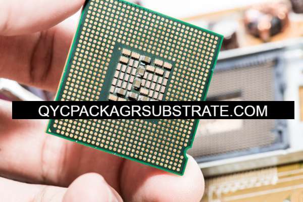
Ball Grid Array Package Substrate
What are the functions of Ball Grid Array Package Substrate?
The Ball Grid Array (BGA) package substrate serves several important functions in electronic devices:
Mechanical Support: The substrate provides a stable platform for mounting the integrated circuit (IC) chip. It ensures that the chip is securely held in place within the package and can withstand mechanical stresses such as vibration and shock.
Electrical Interconnection: The substrate facilitates the electrical connections between the IC chip and the rest of the electronic system. It contains conductive traces that route signals from the chip’s input and output pads to the solder balls or other connection points on the package.
Heat Dissipation: BGA package substrates often include features designed to dissipate heat generated by the IC chip during operation. These features can include thermal vias, thermal pads, or metal heat spreaders that help transfer heat away from the chip and distribute it more evenly across the substrate and surrounding components.
Signal Integrity: The substrate plays a crucial role in maintaining signal integrity by minimizing signal losses, reflections, and crosstalk. It is designed to provide controlled impedance traces and minimize parasitic effects that could degrade signal quality.
Package Sealing and Protection: The substrate can also provide a degree of sealing and protection for the IC chip against environmental factors such as moisture, dust, and contaminants. Some substrates may include coatings or encapsulation materials to enhance durability and reliability.
Overall, the BGA package substrate is essential for ensuring the proper functioning, reliability, and performance of electronic devices by providing mechanical support, electrical connectivity, thermal management, signal integrity, and protection for the integrated circuit chip.
What are the different types of Ball Grid Array Package Substrate?
There are several different types of Ball Grid Array (BGA) package substrates, each with its own characteristics and applications. Some common types include:
Organic Substrates: Organic substrates are made primarily of organic materials such as epoxy resins and fiberglass. They are lightweight, cost-effective, and suitable for most consumer electronics applications. Organic substrates typically offer good electrical performance and thermal characteristics.
Ceramic Substrates: Ceramic substrates are made of ceramic materials such as alumina (Al2O3) or aluminum nitride (AlN). They offer excellent thermal conductivity, mechanical strength, and reliability, making them suitable for high-power applications and harsh operating environments. Ceramic substrates are often used in aerospace, automotive, and military applications.
Flexible Substrates: Flexible substrates are made of flexible materials such as polyimide or liquid crystal polymer (LCP). They are used in applications where bending or flexibility is required, such as wearable devices, flexible displays, and medical electronics.
Metal Core Substrates: Metal core substrates have a metal core layer sandwiched between layers of insulating material. The metal core provides excellent thermal conductivity, allowing for efficient heat dissipation from the IC chip. Metal core substrates are commonly used in high-power LED lighting, automotive electronics, and power electronics applications.
Stacked Substrates: Stacked substrates consist of multiple layers of substrate material stacked on top of each other. Stacked substrates allow for increased routing density and complexity, making them suitable for high-density interconnect (HDI) applications such as advanced microprocessors and high-performance computing.
Advanced Substrate Materials: With advancements in materials science and technology, new types of substrate materials are continually being developed to meet the evolving needs of electronic devices. These materials may offer enhanced electrical performance, thermal properties, reliability, or other characteristics compared to traditional substrates.
These are some of the common types of BGA package substrates, each offering unique advantages and suitability for different applications and requirements.
What is the relationship between Ball Grid Array Package Substrate and IC packaging?
The relationship between Ball Grid Array (BGA) package substrate and integrated circuit (IC) packaging is that the BGA package substrate is a crucial component of the overall IC packaging structure.
IC packaging refers to the process of enclosing an integrated circuit (IC) chip in a protective package that provides mechanical support, electrical connectivity, and thermal management. The IC packaging process typically involves mounting the IC chip onto a substrate, connecting the chip to the substrate using wire bonds or flip-chip technology, encapsulating the assembly in a protective material, and adding external connection points such as pins or solder balls.
The BGA package substrate serves as the foundation for the IC chip within the package. It provides a platform for mounting the chip, facilitates electrical connections between the chip and the rest of the electronic system, helps dissipate heat generated by the chip during operation, and offers protection against environmental factors.
The BGA package substrate is where the solder balls or other connection points are located, which enable the IC package to be mounted onto a printed circuit board (PCB) or other electronic assembly. These solder balls provide the electrical interface between the IC package and the PCB, allowing signals to be transmitted between the IC and the rest of the system.
In summary, the BGA package substrate is an integral part of the IC packaging process, playing a crucial role in providing mechanical support, electrical connectivity, thermal management, and environmental protection for the IC chip within the package.
How does Ball Grid Array Package Substrate differ from PCB?
Ball Grid Array (BGA) package substrate and printed circuit board (PCB) are both essential components in electronic assemblies, but they serve different purposes and have distinct characteristics:
Functionality:
BGA Package Substrate: The primary function of a BGA package substrate is to provide a platform for mounting and connecting an integrated circuit (IC) chip within a package. It facilitates electrical connections between the IC chip and the rest of the electronic system, provides mechanical support for the chip, and helps dissipate heat generated by the chip during operation.
PCB: A PCB serves as a physical foundation for mounting various electronic components, including IC packages, resistors, capacitors, and connectors. It provides electrical connections between components through conductive traces, allowing signals to be routed between different parts of the electronic system. PCBs also provide mechanical support and structural integrity to electronic assemblies.
Composition:
BGA Package Substrate: BGA package substrates are typically made of materials optimized for high-frequency performance, thermal conductivity, and mechanical strength. They often consist of multiple layers of insulating material (such as organic or ceramic substrates) with conductive traces and solder balls for connecting the IC chip to external components.
PCB: PCBs are typically made of layers of fiberglass or other insulating materials laminated with conductive copper traces. They may also include additional layers for power and ground planes, as well as solder mask and silkscreen layers for protection and labeling. PCBs can be rigid, flexible, or rigid-flex depending on the application.
Integration:
BGA Package Substrate: BGA package substrates are integrated directly within IC packages and are designed to accommodate specific chip configurations and requirements. They are manufactured as part of the IC packaging process.
PCB: PCBs are separate components that are designed and manufactured independently of IC packages. They are often customized to fit the specific layout and connectivity needs of a particular electronic assembly, and they can be populated with various components based on the design requirements.
In summary, while both BGA package substrates and PCBs play critical roles in electronic assemblies, they differ in terms of functionality, composition, and integration within the overall system. BGA package substrates are specialized components designed specifically for mounting and connecting IC chips within packages, whereas PCBs provide the foundation for mounting various electronic components and facilitating interconnections within electronic assemblies.
What are the structure and production technology of Ball Grid Array Package Substrate?
The structure and production technology of Ball Grid Array (BGA) package substrates can vary depending on factors such as the substrate material (e.g., organic, ceramic), the specific requirements of the integrated circuit (IC) chip, and the desired performance characteristics. However, here is a general overview of the structure and production technology of BGA package substrates:
Structure:
Base Material: BGA package substrates are typically made of insulating materials such as organic resins (e.g., epoxy) or ceramics (e.g., alumina, aluminum nitride). The choice of base material depends on factors such as thermal conductivity, electrical performance, and mechanical strength requirements.
Conductive Traces: Multiple layers of conductive traces (usually made of copper) are patterned onto the substrate material using processes such as photolithography and etching. These traces route electrical signals between the IC chip and the solder balls or other connection points on the package.
Solder Balls: Solder balls are attached to the bottom surface of the substrate using techniques such as solder ball placement, reflow soldering, or solder paste printing. These solder balls serve as the interface between the IC chip and the printed circuit board (PCB) or other external components, providing electrical connectivity and mechanical attachment.
Surface Finish: The surface of the substrate may be finished with a layer of solder mask or other protective coatings to prevent oxidation, contamination, and electrical shorting between conductive traces.
Production Technology:
Substrate Fabrication: The fabrication of BGA package substrates typically involves processes such as lamination, drilling, and metallization. For organic substrates, layers of insulating material are laminated together, and holes are drilled to create vias for interconnecting traces between different layers. Ceramic substrates may undergo processes such as green machining, firing, and metallization to achieve the desired structure and properties.
Conductive Traces Patterning: Conductive traces are patterned onto the substrate material using photolithography and etching techniques. A layer of photoresist is applied to the substrate, exposed to UV light through a photomask, and developed to create a pattern for the traces. The exposed areas are then etched away to leave behind the desired conductive traces.
Solder Ball Attachment: Solder balls are attached to the substrate using processes such as solder ball placement, reflow soldering, or solder paste printing. In reflow soldering, solder balls are placed onto pre-defined pads on the substrate, and the assembly is heated in a reflow oven to melt the solder and form a reliable electrical connection.
Quality Assurance: BGA package substrates undergo rigorous quality assurance testing to ensure that they meet specifications for electrical performance, mechanical strength, and reliability. This may include visual inspection, electrical testing, thermal cycling, and other reliability tests to verify the integrity of the substrate and its solder connections.
Overall, the production technology of BGA package substrates involves a combination of materials processing, patterning, and assembly techniques to create substrates that meet the electrical, mechanical, and thermal requirements of the IC package and the electronic system.
Frequently Asked Questions (FAQs)
What is a BGA package substrate?
A BGA package substrate is a component of integrated circuit packaging used to mount and connect IC chips within packages. It provides mechanical support, electrical connectivity, and thermal management for the IC chip.
What materials are used to make BGA package substrates?
BGA package substrates can be made from various materials, including organic resins (e.g., epoxy), ceramics (e.g., alumina, aluminum nitride), and metal-core materials. The choice of material depends on factors such as thermal conductivity, electrical performance, and mechanical strength requirements.
What are the advantages of BGA package substrates?
BGA package substrates offer several advantages over other packaging technologies, including higher pin counts, better thermal performance, reduced size and weight, and improved reliability. They are widely used in a variety of electronic devices, including computers, smartphones, and networking equipment.
How are BGA package substrates manufactured?
The manufacturing process for BGA package substrates typically involves processes such as substrate fabrication, conductive trace patterning, solder ball attachment, and quality assurance testing. These processes may vary depending on factors such as the substrate material and specific requirements of the IC chip.
What are the key considerations when selecting a BGA package substrate?
When selecting a BGA package substrate, key considerations include the material properties (e.g., thermal conductivity, electrical performance), the substrate thickness and size, the number and arrangement of solder balls, and compatibility with the IC chip and the overall electronic system.
What are some common failure modes of BGA package substrates?
Common failure modes of BGA package substrates include solder ball cracking, delamination, and electrical open or short circuits. These failures can be caused by factors such as thermal cycling, mechanical stress, or manufacturing defects.
How can BGA package substrate reliability be improved?
BGA package substrate reliability can be improved through design optimization, material selection, manufacturing process improvements, and rigorous quality assurance testing. Techniques such as thermal management, underfill encapsulation, and solder joint reinforcement can also enhance substrate reliability.
Conclusion
In conclusion, Ball Grid Array (BGA) package substrates play a critical role in the packaging of integrated circuits (ICs), providing essential functions such as mechanical support, electrical connectivity, thermal management, and environmental protection for the IC chip within the package. These substrates are manufactured using a combination of materials processing, patterning, and assembly techniques, and they come in various types and configurations to suit different applications and requirements. Despite their importance, BGA package substrates are just one component in the complex ecosystem of electronic assemblies, and their reliability and performance depend on factors such as material selection, design optimization, manufacturing quality, and environmental conditions. By understanding the structure, production technology, and key considerations related to BGA package substrates, electronics designers and manufacturers can make informed decisions to ensure the reliability, functionality, and longevity of electronic devices and systems.