
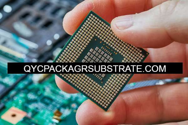
What is CSP Package Substrate?
CSP Package and CSP Package Substrate Firm . the Package Substrate will be made with Showa Denko and Ajinomoto High speed materials.or other types high speed materials and high frequency materials.
CSP (Chip Scale Package) substrate refers to the substrate material used in the construction of semiconductor chips. It is a critical component in the packaging process of integrated circuits. The substrate serves as a foundation for mounting and connecting the various components of the chip, such as the semiconductor die, wire bonds, and solder balls.
CSP substrates are designed to be as small as possible, hence the term “chip scale,” meaning that the package size is comparable to the size of the semiconductor die itself. This allows for more efficient use of space on printed circuit boards (PCBs) and enables the production of smaller, more compact electronic devices.
The substrate material used in CSP packages is typically a laminate composed of layers of different materials, such as fiberglass-reinforced epoxy resin. These materials provide the necessary electrical and mechanical properties required for reliable performance in a variety of applications.
CSP packages offer several advantages over traditional packaging methods, including reduced size and weight, improved electrical performance, and enhanced thermal management. These benefits make CSP substrates popular choices for a wide range of semiconductor devices, including mobile phones, tablets, wearables, and other portable electronics.
CSP Package Substrate
What are the functions of CSP Package Substrate?
CSP (Chip Scale Package) package substrate serves several key functions in the packaging of semiconductor chips:
Mounting Surface: The substrate provides a surface for mounting the semiconductor die (the actual chip) and other components such as passive devices (resistors, capacitors) and active devices (transistors).
Electrical Interconnection: It facilitates electrical connections between the semiconductor die and other components through wire bonds or flip-chip connections. These connections enable the flow of electrical signals between different parts of the chip and external circuitry.
Thermal Management: The substrate helps dissipate heat generated by the semiconductor die during operation. It may include features such as thermal vias, copper traces, or heat spreaders to efficiently transfer heat away from the chip to the surrounding environment.
Mechanical Support: The substrate provides structural support for the semiconductor die and other components, ensuring their proper alignment and protection from mechanical stresses such as bending or vibration.
Signal Integrity: It contributes to maintaining signal integrity by minimizing signal loss, noise, and impedance mismatches within the package and between the package and external components.
Overall, the CSP package substrate plays a crucial role in the performance, reliability, and manufacturability of semiconductor devices by providing a platform for integrating and connecting various components while ensuring efficient thermal management and signal transmission.
What are the different types of CSP Package Substrate?
There are several types of CSP (Chip Scale Package) package substrates, each with its own characteristics and advantages. Some common types include:
Organic Substrates: These are made of organic materials such as epoxy resin or polyimide. Organic substrates are lightweight, cost-effective, and offer good electrical insulation properties. They are widely used in consumer electronics and mobile devices.
Ceramic Substrates: Ceramic substrates are made of materials such as alumina (aluminum oxide) or aluminum nitride. They offer excellent thermal conductivity and mechanical stability, making them suitable for high-power applications and environments with demanding thermal requirements.
Silicon Substrates: Silicon substrates are typically used in flip-chip CSP packages, where the semiconductor die is directly mounted onto a silicon wafer. Silicon substrates offer high electrical conductivity and compatibility with standard semiconductor manufacturing processes.
Glass Substrates: Glass substrates provide excellent electrical insulation properties and are suitable for applications requiring high reliability and miniaturization. They are commonly used in optoelectronic devices and bio-sensors.
Metal Substrates: Metal substrates, such as copper or aluminum, are used in CSP packages that require superior thermal conductivity and heat dissipation capabilities. They are commonly used in high-power LED modules, automotive electronics, and power electronics.
Flexible Substrates: Flexible substrates, made of materials like polyimide or liquid crystal polymer (LCP), are used in flexible or bendable electronic devices. They offer flexibility and conformability, making them suitable for applications such as wearable electronics and flexible displays.
These are just a few examples of the types of CSP package substrates available, and each type may offer unique advantages depending on the specific requirements of the application.
What is the relationship between CSP Package Substrate and IC packaging?
CSP (Chip Scale Package) package substrate is a critical component within the broader context of IC (Integrated Circuit) packaging. IC packaging involves the process of encapsulating and protecting semiconductor chips (ICs) while providing electrical connections to external circuitry. The CSP package substrate plays a crucial role in this process by providing a foundation for mounting and interconnecting the various components of the semiconductor chip.
Here’s how CSP package substrate relates to IC packaging:
Mounting Surface: The substrate serves as a mounting surface for the semiconductor die (the actual chip) and other components such as passive devices (resistors, capacitors) and active devices (transistors). These components are attached to the substrate using techniques such as wire bonding or flip-chip bonding.
Electrical Interconnection: The substrate facilitates electrical connections between the semiconductor die and external circuitry. It contains conductive traces and pads that enable the flow of electrical signals between the chip and other components on the substrate, as well as connections to the outside world via solder balls or other interconnection methods.
Thermal Management: The substrate helps dissipate heat generated by the semiconductor die during operation. It may include features such as thermal vias, copper traces, or heat spreaders to efficiently transfer heat away from the chip to the surrounding environment, thereby preventing overheating and ensuring proper functioning of the device.
Signal Integrity: The substrate plays a role in maintaining signal integrity by minimizing signal loss, noise, and impedance mismatches within the package and between the package and external components. This is achieved through careful design of the substrate layout and material selection to minimize parasitic effects.
Overall, the CSP package substrate is an integral part of the IC packaging process, contributing to the performance, reliability, and manufacturability of semiconductor devices. It provides a platform for integrating and connecting various components while ensuring efficient thermal management and signal transmission, ultimately enabling the functionality of the packaged IC.
How does CSP Package Substrate differ from PCB?
CSP (Chip Scale Package) package substrate and PCB (Printed Circuit Board) are both essential components in electronic devices, but they serve different purposes and have distinct characteristics. Here are some key differences between CSP package substrates and PCBs:
Function:
CSP Package Substrate: The primary function of a CSP package substrate is to provide a platform for mounting and interconnecting the components of a semiconductor chip (IC). It serves as a foundation for the semiconductor die and other components, facilitating electrical connections and providing thermal management.
PCB: A PCB is a complete board that provides mechanical support and electrical interconnection for electronic components. It serves as a base for mounting various components such as ICs, resistors, capacitors, and connectors, and it facilitates electrical connections between these components through conductive traces etched on its surface.
Size and Scale:
CSP Package Substrate: CSP package substrates are typically smaller and more compact compared to PCBs. They are designed to be as close in size to the semiconductor die as possible, hence the term “chip scale.”
PCB: PCBs can vary widely in size, depending on the specific application and the number and size of components mounted on them. They can range from small, densely populated boards used in consumer electronics to larger boards used in industrial equipment.
Material and Construction:
CSP Package Substrate: CSP package substrates are often made of materials such as organic laminates, ceramics, silicon, or metal, depending on the specific requirements of the application. They are typically designed to provide excellent electrical properties, thermal conductivity, and mechanical stability.
PCB: PCBs are usually made of layers of fiberglass-reinforced epoxy resin, known as FR4, although other materials such as flexible substrates or metal core substrates may also be used. PCBs may incorporate additional features such as solder mask and silkscreen for labeling and protection.
Application:
CSP Package Substrate: CSP package substrates are primarily used in semiconductor packaging, where space and weight considerations are critical, such as in mobile devices, wearables, and other compact electronic devices.
PCB: PCBs are used in a wide range of electronic devices and applications, including computers, consumer electronics, automotive systems, medical devices, and industrial equipment.
Overall, while both CSP package substrates and PCBs play crucial roles in electronic devices, they differ in their function, size, material, and application, reflecting the specific requirements and constraints of the systems they are designed for.
What are the structure and production technology of CSP Package Substrate?
The structure and production technology of CSP (Chip Scale Package) package substrates can vary depending on the specific design requirements and materials used. However, here is a general overview of the structure and production process:
Structure:
Base Material: CSP package substrates are typically constructed from a base material that provides the foundation for the substrate. Common base materials include organic substrates (e.g., epoxy resin, polyimide), ceramic substrates (e.g., alumina, aluminum nitride), silicon substrates, glass substrates, metal substrates (e.g., copper, aluminum), or flexible substrates (e.g., polyimide, liquid crystal polymer).
Conductive Traces and Pads: The substrate contains conductive traces and pads made of metals such as copper or aluminum. These traces and pads provide electrical connections between the semiconductor die and other components, as well as connections to external circuitry.
Insulating Layers: Insulating layers are used to separate conductive traces and pads, preventing electrical shorts and ensuring proper signal routing. These layers are typically made of materials such as epoxy resin, polyimide, or other dielectric materials.
Thermal Management Features: CSP package substrates may include thermal management features such as thermal vias, copper traces, or heat spreaders to dissipate heat generated by the semiconductor die during operation and maintain optimal operating temperatures.
Production Technology:
Substrate Manufacturing: The production process begins with the manufacturing of the substrate base material. Depending on the type of substrate, this may involve processes such as lamination, deposition, etching, or machining to create the desired substrate structure.
Layer Build-Up: Conductive traces, pads, and insulating layers are then deposited or patterned onto the substrate base material using techniques such as lithography, etching, or screen printing. Multiple layers may be built up to create complex substrate structures.
Via Formation: Thermal vias or electrical vias may be created by drilling or laser ablation to provide pathways for heat dissipation or electrical connections between different layers of the substrate.
Surface Finish: The substrate surface is typically finished with a layer of metal (e.g., solder, gold) to facilitate soldering or wire bonding of semiconductor chips and other components.
Testing and Inspection: The finished CSP package substrates undergo testing and inspection to ensure they meet the required specifications for electrical performance, thermal management, and reliability.
Overall, the production technology of CSP package substrates involves a combination of materials processing, patterning, and assembly techniques to create substrates that meet the stringent requirements of modern semiconductor packaging.
Frequently Asked Questions (FAQs)
What is a CSP package substrate?
A CSP package substrate is a key component in the packaging of semiconductor chips. It serves as a foundation for mounting and interconnecting the various components of the chip, including the semiconductor die, wire bonds, and solder balls.
What are the functions of CSP package substrates?
CSP package substrates perform several functions, including providing a mounting surface for the semiconductor die and other components, facilitating electrical interconnections, managing thermal dissipation, providing mechanical support, and maintaining signal integrity.
What are the different types of CSP package substrates?
Common types of CSP package substrates include organic substrates (e.g., epoxy resin, polyimide), ceramic substrates (e.g., alumina, aluminum nitride), silicon substrates, glass substrates, metal substrates (e.g., copper, aluminum), and flexible substrates (e.g., polyimide, liquid crystal polymer).
How are CSP package substrates produced?
The production process of CSP package substrates involves manufacturing the substrate base material, building up layers of conductive traces, pads, and insulating layers, forming thermal vias or electrical vias, finishing the substrate surface, and conducting testing and inspection to ensure quality and reliability.
What are the advantages of CSP package substrates?
CSP package substrates offer advantages such as smaller size and weight, improved electrical performance, enhanced thermal management, and higher reliability compared to traditional packaging methods. They enable the production of smaller, more compact electronic devices with improved functionality.
What applications are CSP package substrates used in?
CSP package substrates are used in a wide range of semiconductor devices, including mobile phones, tablets, wearables, automotive electronics, medical devices, and industrial equipment. They are particularly well-suited for applications requiring miniaturization, high reliability, and efficient thermal management.
Conclusion
In conclusion, CSP (Chip Scale Package) package substrates are essential components in the packaging of semiconductor chips, serving multiple functions such as providing a mounting surface, facilitating electrical connections, managing thermal dissipation, offering mechanical support, and maintaining signal integrity. They come in various types, including organic, ceramic, silicon, glass, metal, and flexible substrates, each with its unique advantages and applications.
The production process of CSP package substrates involves manufacturing the substrate base material, building up layers of conductive traces and insulating layers, forming vias, finishing the substrate surface, and conducting testing and inspection to ensure quality and reliability.
CSP package substrates offer numerous benefits, including smaller size and weight, improved electrical performance, enhanced thermal management, and higher reliability compared to traditional packaging methods. They find applications in a wide range of electronic devices, including mobile phones, tablets, wearables, automotive electronics, medical devices, and industrial equipment.
Overall, CSP package substrates play a crucial role in enabling the development of smaller, more compact electronic devices with improved functionality, making them indispensable in the semiconductor industry.