
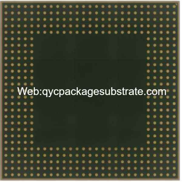
What Defines FC-BGA Substrates?
Package substrate and FC-BGA Substrate manufacturer. We use advanced Msap and Sap technology, High multilayer interconnection substrates from 4 to 20 layers. High quality base materials and fast lead time.
FCBGA (Flip-Chip Ball Grid Array) substrates represent a packaging technology utilized in integrated circuits (ICs) and microprocessors. Distinguished by a unique design, they confer various advantages in terms of performance, size, and reliability. Here are some key features that define FCBGA substrates and contribute to their significance in modern PCB (Printed Circuit Board) engineering:
-
Flip-Chip Technology:
-
- FCBGA utilizes flip-chip technology, where the semiconductor die is flipped and mounted face down on the substrate. This is in contrast to traditional packaging methods where the chip is mounted upright.
-
Ball Grid Array (BGA):
-
- FCBGA incorporates a ball grid array, which consists of an array of solder balls on the underside of the package. These solder balls provide electrical connections between the chip and the PCB.
-
Reduced Inductance and Parasitic Effects:
-
- The flip-chip design of FCBGA substrates allows for shorter and more direct electrical paths between the chip and the PCB. This reduces inductance and parasitic effects, leading to improved electrical performance.
-
Higher Density Packaging:
-
- FCBGA allows for higher packaging density compared to traditional packaging methods. The flip-chip design enables a more compact arrangement of components, contributing to the miniaturization of electronic devices.
-
Improved Thermal Performance:
-
- The flip-chip design also enhances thermal performance by allowing for better heat dissipation. The direct attachment of the chip to the substrate facilitates efficient heat transfer, which is crucial for preventing overheating and maintaining the reliability of the device.
-
Enhanced Signal Integrity:
-
- The shorter interconnects in FCBGA substrates contribute to improved signal integrity. Reduced signal delays and minimized crosstalk between adjacent traces result in better overall performance of the integrated circuit.
-
Advanced Manufacturing Processes:
-
- FCBGA substrates often involve advanced manufacturing processes, such as high-density interconnect (HDI) technology and precision assembly techniques. These processes contribute to the overall reliability and performance of the packaged IC.
-
Compatibility with High-Frequency Applications:
- The design of FCBGA substrates makes them suitable for high-frequency applications. The reduced parasitic effects and improved signal integrity make them ideal for use in devices with high-speed data transmission requirements.
In summary, FCBGA substrates stand out in modern PCB engineering due to their flip-chip design, ball grid array configuration, and associated benefits such as higher packaging density, improved thermal performance, and enhanced signal integrity. These characteristics make FCBGA a valuable technology for meeting the demands of contemporary electronic devices, especially those requiring compact size, high performance, and reliability.
What Functions Do FC-BGA Substrates Serve?
FCBGA (Flip-Chip Ball Grid Array) substrates serve multiple critical functions beyond being a platform for bottom-level connections. Their design and characteristics contribute to enhanced performance and reliability in various aspects, including heat dissipation, electrical signal transmission, and power management. Here’s an overview of the functions that FCBGA substrates serve:
-
Bottom-Level Connections:
-
- FCBGA substrates provide a platform for the bottom-level connections of an integrated circuit. The solder balls on the underside of the package facilitate electrical connections between the semiconductor die and the printed circuit board (PCB).
-
Heat Dissipation:
-
- The flip-chip design of FCBGA substrates allows for efficient heat dissipation. By directly attaching the semiconductor die to the substrate, heat generated during operation can be more effectively transferred away from the chip, preventing overheating and maintaining optimal operating temperatures.
-
Electrical Signal Transmission:
-
- FCBGA substrates contribute to improved electrical signal transmission. The shorter and more direct electrical paths between the chip and the PCB reduce signal delays, enhance signal integrity, and minimize crosstalk between adjacent traces. This is particularly crucial for high-speed and high-frequency applications.
-
High Packaging Density:
-
- FCBGA enables higher packaging density due to its compact design. The flip-chip arrangement allows for a more efficient use of space, accommodating more components in a smaller footprint. This is essential for devices where miniaturization is a key requirement.
-
Reduced Inductance and Parasitic Effects:
-
- The flip-chip design minimizes inductance and parasitic effects. Shorter interconnects result in lower electrical resistance and better overall performance, especially in applications where high-frequency operation is essential.
-
Power Management:
-
- FCBGA substrates contribute to effective power management. The improved thermal performance and reduced power losses associated with the design help optimize power consumption, enhancing the overall energy efficiency of the integrated circuit.
-
Reliability Enhancement:
- The advanced manufacturing processes and materials used in FCBGA substrates contribute to their reliability. The robust electrical connections, efficient heat dissipation, and minimized signal interference collectively enhance the overall reliability of the packaged IC.
In summary, FCBGA substrates serve as more than just a platform for connections. They play a crucial role in heat dissipation, electrical signal transmission, power management, and reliability, making them a valuable technology in modern integrated circuit packaging.
What Types of FC/BGA Substrates Exist?
There are several types of FCBGA (Flip-Chip Ball Grid Array) substrates, each designed to meet specific requirements in different application scenarios. The variations in FCBGA substrates may involve differences in materials, design features, or specific technologies applied. Here are some common types and considerations:
-
Standard FCBGA:
-
- Advantages: Standard FCBGA substrates present a cost-efficient and extensively adopted solution across various applications. They deliver a well-balanced combination of performance and reliability.
- Disadvantages:In high-performance or specialized applications, standard FCBGA substrates may encounter challenges related to thermal performance or signal integrity.
-
Enhanced Thermal FCBGA:
-
- Advantages: These substrates are specifically designed to optimize thermal performance. They may include advanced heat dissipation technologies, such as enhanced materials or additional features to improve cooling.
- Disadvantages: Enhanced thermal FCBGA substrates might be more expensive than standard versions. However, the improved thermal management can be crucial for applications with stringent heat dissipation requirements.
-
High-Density Interconnect (HDI) FCBGA:
-
- Advantages: HDI FCBGA substrates utilize advanced manufacturing processes to achieve higher packaging density. This is beneficial for applications where miniaturization and component density are critical.
- Disadvantages: The manufacturing complexity of HDI FCBGA substrates may result in higher production costs. Additionally, the increased density may pose challenges in terms of signal integrity and thermal management.
-
Power Delivery Network (PDN) Optimized FCBGA:
-
- Advantages: These substrates are designed to optimize power delivery, ensuring stable and efficient power distribution across the integrated circuit. This is particularly important for applications with varying power requirements.
- Disadvantages: PDN-optimized FCBGA substrates may have specific design considerations that could impact other aspects of performance, and they may be tailored to certain applications.
-
Fine-Pitch FCBGA:
- Advantages: Fine-pitch FCBGA substrates have a smaller pitch between the solder balls, allowing for higher interconnect density. This is advantageous in applications where space is a premium.
- Disadvantages: The finer pitch may pose challenges during manufacturing and assembly, potentially leading to increased production costs. It may also introduce challenges in terms of reliability and robustness.
How Are FC BGA Substrates Connected to PCBs?
FCBGA (Flip-Chip Ball Grid Array) substrates play a vital role in connecting semiconductor chips to printed circuit boards (PCBs). The connection process involves specific steps that integrate the FCBGA substrate into the overall PCB engineering process. Here’s an overview of how FCBGA substrates are connected to PCBs:
-
Flip-Chip Mounting:
-
- The first step involves mounting the semiconductor chip onto the FCBGA substrate using flip-chip technology. In this process, the chip is flipped and attached face-down onto the substrate, and it is typically connected using solder bumps.
-
Solder Ball Array:
-
- The underside of the FCBGA substrate features a grid array of solder balls. These solder balls serve as the primary electrical connections between the chip and the PCB. The number and arrangement of solder balls depend on the specific design and requirements of the application.
-
Alignment and Reflow Soldering:
-
- The FCBGA substrate, with the chip attached and solder balls in place, is aligned with corresponding pads on the PCB. The entire assembly is then subjected to a reflow soldering process. During reflow soldering, the solder balls melt and form secure connections with the PCB pads.
-
Connection to PCB:
-
- Once the reflow soldering process is complete, the FCBGA substrate is securely connected to the PCB. The solder balls create electrical connections, and the mechanical attachment ensures stability. The close proximity of the chip to the PCB contributes to the overall compactness and efficiency of the electronic device.
-
Integration with Other Components:
-
- The PCB, with the attached FCBGA substrate, is part of the larger system.Supplementary electronic elements, including resistors, capacitors, and additional chips, can be affixed to the PCB to finalize the circuit and deliver the required functionalities.
-
Testing and Quality Assurance:
-
- The integrated assembly undergoes testing to ensure the functionality and reliability of the connections. Various testing methods, such as electrical testing and thermal testing, may be employed to verify the performance of the FCBGA package on the PCB.
-
Adaptability to Different Board Sizes and Shapes:
- FCBGA substrates are adaptable to different PCB sizes and shapes. The compact design and high packaging density make them suitable for applications where space is limited. The scalability of FCBGA technology allows it to be utilized in a variety of electronic devices, ranging from small consumer gadgets to larger industrial equipment.
In summary, FCBGA substrates are closely connected to PCBs through a process that involves flip-chip mounting, solder ball arrays, alignment, reflow soldering, and integration with other components. This connection method allows for efficient and reliable packaging of semiconductor chips onto PCBs, making FCBGA technology applicable to a wide range of circuit board sizes and shapes.
What Comprises the Main Structure and Production Technologies of FC/BGA Substrates?
The main structure of FCBGA (Flip-Chip Ball Grid Array) substrates comprises several key components, and their production involves advanced manufacturing technologies, particularly in the realm of High-Density Interconnect (HDI). Here’s an overview of the main components and production technologies of FCBGA substrates:
Components of FCBGA Substrates:
-
Substrate Material:
-
- The substrate material is typically a high-performance laminate or organic material. It provides the structural foundation for the FCBGA substrate.
-
Conductive Layers:
-
- FCBGA substrates have multiple conductive layers, including signal layers and power distribution layers. These layers facilitate the routing of electrical signals and power to and from the flip-chip.
-
Dielectric Layers:
-
- Dielectric layers, typically composed of materials exhibiting low electrical conductivity, serve to isolate the conductive layers, mitigating the risk of short circuits. The selection of dielectric material plays a pivotal role in shaping the electrical characteristics of the substrate.
-
Solder Mask:
-
- Solder mask is applied over the conductive layers to insulate and protect the copper traces from environmental factors. It also defines the areas where soldering will occur.
-
Copper Traces and Pads:
-
- Copper traces and pads form the electrical pathways on the FCBGA substrate. These are designed to route signals, power, and ground connections to and from the flip-chip.
-
Solder Balls:
- The underside of the FCBGA substrate features an array of solder balls. These solder balls act as the interconnects between the substrate and the PCB.
Production Technologies of FCBGA Substrates:
-
High-Density Interconnect (HDI) Manufacturing:
-
- HDI manufacturing processes are integral to FCBGA substrate production. HDI involves the use of advanced techniques to achieve higher circuit density and more compact designs. This includes microvias, laser drilling, and fine-line technology to create intricate and densely packed structures.
-
Microvias:
-
- Microvias are small, laser-drilled holes used to connect different layers of the substrate. They contribute to the miniaturization of the circuit and enhance the overall density.
-
Laser Drilling:
-
- Laser drilling is a precise method used to create small holes for microvias. It allows for finer control over the size and placement of vias, supporting the high-density requirements of FCBGA substrates.
-
Fine-Line Technology:
-
- Fine-line technology involves the creation of narrow and closely spaced traces on the substrate. This allows for more intricate routing of signals and power, accommodating the demand for compact designs in FCBGA substrates.
-
Improved Semi-Additive Methods:
- Semi-additive methods involve selectively depositing and patterning metal on the substrate. Improved semi-additive methods enhance the precision and resolution of metal deposition, contributing to the manufacturing of fine features on the substrate.
Practical Application of Improved Semi-Additive Methods:
-
Precision Metal Deposition:
-
- Advanced semi-additive methods allow for precise and controlled deposition of metal, enabling the creation of fine features such as narrow traces and pads.
-
Enhanced Resolution:
-
- Improved semi-additive techniques enhance the resolution of the manufacturing process, ensuring that intricate details and fine structures can be accurately produced on the substrate.
-
High-Quality Circuit Formation:
- The practical application of improved semi-additive methods results in high-quality circuit formation on FCBGA substrates, contributing to the overall performance and reliability of the integrated circuits.
In summary, the main structure of FCBGA substrates includes substrate material, conductive layers, dielectric layers, solder mask, copper traces and pads, and solder balls. The production technologies involve High-Density Interconnect (HDI) manufacturing techniques, microvias, laser drilling, fine-line technology, and improved semi-additive methods, all of which contribute to the superior performance and miniaturization capabilities of FCBGA substrates.
What Common Questions Arise Regarding FC BGA Substrates?
What is FCBGA?
Understanding the basics is crucial. Providing a clear definition of FCBGA, its full form (Flip-Chip Ball Grid Array), and its role in semiconductor packaging helps set the foundation for further exploration.
How Does FCBGA Differ from Other Packaging Technologies?
Readers may want to know how FCBGA compares to other packaging technologies, such as Quad Flat Packages (QFP) or Chip-on-Board (COB). Addressing these differences can help readers appreciate the unique features and advantages of FCBGA.
What Are the Advantages of FCBGA Substrates?
Explaining the specific advantages, such as enhanced thermal performance, high-density packaging, and improved signal integrity, helps readers understand why FCBGA is preferred in certain applications.
How Does FCBGA Contribute to Miniaturization?
Readers might be interested in understanding how the flip-chip design and other features of FCBGA substrates contribute to the miniaturization of electronic devices.
What Applications Benefit Most from FCBGA?
Addressing the specific applications where FCBGA excels, such as high-performance computing, telecommunications, or consumer electronics, helps readers identify scenarios where this technology is most beneficial.
How Are FCBGA Substrates Connected to PCBs?
Explaining the connection process, including flip-chip mounting, solder ball arrays, and reflow soldering, provides insights into the integration of FCBGA substrates with printed circuit boards.
What Challenges Exist with FCBGA Technology?
Acknowledging potential challenges, such as manufacturing complexity or increased production costs, helps readers make informed decisions and consider alternatives based on their specific requirements.
Are FCBGA Substrates Suitable for High-Frequency Applications?
Readers may inquire about the compatibility of FCBGA substrates with high-frequency applications. Clarifying their suitability for such scenarios, along with details on signal integrity, is important.
What Manufacturing Technologies Are Involved in FCBGA Production?
Providing insights into the manufacturing processes, including High-Density Interconnect (HDI), laser drilling, and improved semi-additive methods, helps readers understand the technological aspects behind FCBGA production.
How Can FCBGA Substrates Be Tested for Reliability?
Addressing the testing procedures for FCBGA substrates, such as electrical testing and thermal testing, offers readers a perspective on ensuring the reliability of the final product.
Can FCBGA Substrates Truly Drive Innovation in PCB Engineering?
FCBGA (Flip-Chip Ball Grid Array) substrates indeed play a significant role in driving innovation in PCB (Printed Circuit Board) engineering, and their key advantages contribute to their indispensability in certain applications. Here are ways in which FCBGA substrates foster innovation in PCB engineering:
-
High-Density Packaging:
-
- FCBGA substrates offer high-density packaging, allowing for the integration of more components in a smaller footprint. This is crucial for the development of compact and space-efficient electronic devices, driving innovation in miniaturization.
-
Enhanced Thermal Performance:
-
- The flip-chip design of FCBGA substrates facilitates better heat dissipation compared to traditional packaging methods. This advantage is particularly valuable in high-performance applications, such as data centers and high-end computing, where effective thermal management is critical.
-
Improved Signal Integrity:
-
- The short and direct paths between the flip-chip and the PCB, enabled by FCBGA substrates, contribute to improved signal integrity. This is essential for high-speed data transmission and processing, making FCBGA technology suitable for applications demanding robust signal performance.
-
Advanced Manufacturing Technologies:
-
- The use of advanced manufacturing technologies, such as High-Density Interconnect (HDI), microvias, and fine-line technology in FCBGA production, supports intricate and densely packed circuit designs. These technologies enable the creation of highly sophisticated electronic products.
-
Optimized Power Delivery:
-
- Some FCBGA substrates are designed with a focus on optimizing power delivery networks (PDN). This ensures stable and efficient distribution of power across the integrated circuit, which is crucial for applications with varying power requirements.
-
Application in High-Performance Computing:
-
- FCBGA substrates play a pivotal role in high-performance computing environments, significantly contributing to advancements in artificial intelligence, machine learning, and data analytics.Their capacity to manage substantial data loads and efficiently dissipate heat is instrumental in pushing the boundaries of computational capabilities.
-
Versatility Across Industries:
-
- The versatility of FCBGA technology allows it to be applied across various industries, from consumer electronics to telecommunications and automotive systems. Its adaptability makes it a driving force behind innovations in diverse electronic products.
-
Potential for Integration with Emerging Technologies:
-
- As emerging technologies, such as 5G, IoT (Internet of Things), and edge computing, continue to evolve, FCBGA substrates provide a platform for integrating these technologies into compact and high-performance electronic devices. This integration contributes to the advancement of smart and interconnected systems.
-
Reliability and Performance in Harsh Environments:
- FCBGA substrates, with their robust design and efficient heat dissipation capabilities, contribute to the development of reliable electronic products that can perform in harsh environments. This is particularly relevant in industrial and automotive applications.
In conclusion, FCBGA substrates possess key advantages, including high-density packaging, enhanced thermal performance, and improved signal integrity, making them indispensable in driving innovation in PCB engineering. The ongoing development of this advanced technology continues to open up broader prospects for the future of electronic products, enabling more compact, efficient, and high-performance devices across various industries.