
What is the FCBGA Package Substrates?
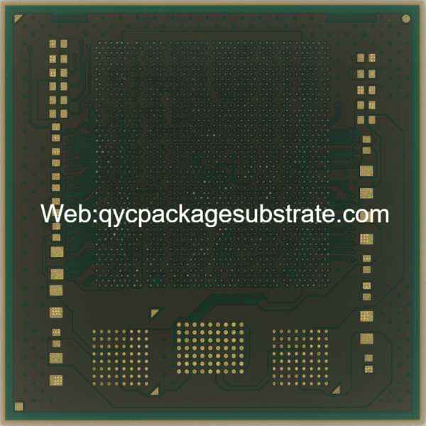
FCBGA Package Substrate production. we can produce the best samllest bump pitch with 100um, the best smallest microtrace are 9um. and the smallest gap are 9um. most of the microtrace design are 15um to 30um trace and spacing.
FCBGA stands for Flip-Chip Ball Grid Array, and it refers to a type of integrated circuit (IC) package used in semiconductor packaging. Here are the fundamental concepts and characteristics that make up the FCBGA package, along with the role of Flip-Chip technology:
Flip-Chip Technology:
Flip-Chip Bonding: In traditional packaging, the semiconductor die is mounted upright on the package substrate, with wire bonds connecting the die to the substrate. In flip-chip technology, the die is flipped upside down, and its active side is directly bonded to the package substrate. This reduces the distance between the die and the substrate, improving electrical performance.
Bump Connections: Tiny solder bumps, known as C4 (controlled collapse chip connection) or solder balls, are deposited on the active side of the semiconductor die. These bumps serve as the electrical and mechanical connections between the die and the substrate.
FCBGA Package Characteristics:
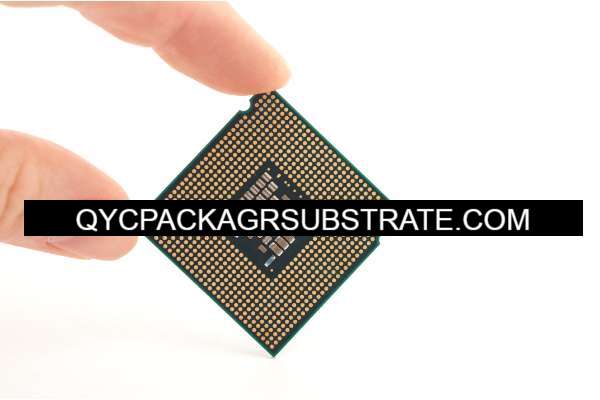
Ball Grid Array (BGA): FCBGA belongs to the Ball Grid Array family of packages. The bottom side of the package contains an array of solder balls that serve as the external connections to the circuit board.
Compact Design: Flip-chip technology allows for a more compact design since the direct connection between the die and substrate reduces the length of the interconnects, leading to shorter signal paths and improved electrical performance.
Thermal Performance: The flip-chip design also enhances thermal performance by allowing for more efficient heat dissipation. Heat generated by the die can be directly transferred to the package substrate and then to the circuit board.
Advantages of FCBGA:
High Performance: The shorter interconnects in FCBGA packages contribute to higher signal integrity and faster data transfer rates.
Reduced Inductance: Because of the direct connection between the die and the substrate, inductance is minimized, leading to better high-frequency performance.
Space Efficiency: FCBGA packages are more space-efficient than some other packaging technologies, making them suitable for applications where board real estate is a critical factor.
Improved Thermal Management: The flip-chip design allows for better heat dissipation, contributing to improved thermal management.
In summary, the FCBGA package combines the advantages of flip-chip technology with the Ball Grid Array packaging format. Recognized for its streamlined design, enhanced electrical capabilities, and effective heat dissipation, the FCBGA emerges as the favored option for cutting-edge semiconductor devices demanding high performance.
What Functions Does the FCBGA Package Serve?
The FCBGA package serves several crucial functions in electronic devices, particularly excelling in high-performance chip packaging:
Electrical Interconnection:
FCBGA facilitates the electrical connection between the semiconductor die and the external circuitry. The flip-chip design with solder bumps ensures efficient and reliable electrical interconnection, contributing to enhanced signal integrity.
Signal Transmission:
By minimizing the length of interconnects, FCBGA reduces signal propagation delays. This is crucial for high-speed and high-frequency applications, allowing for rapid and efficient transmission of signals within the semiconductor device.
Compact Packaging:
FCBGA’s compact design optimizes space utilization on the circuit board. This is particularly advantageous in electronic devices where miniaturization is essential, allowing for more components to be integrated into a smaller footprint.
Thermal Management:
The flip-chip configuration enables efficient dissipation of heat generated by the semiconductor die. This is vital for maintaining optimal operating temperatures and preventing thermal issues that could affect the performance and reliability of the electronic device.
High-Speed Data Processing:
With reduced interconnect lengths and improved signal integrity, FCBGA is well-suited for applications requiring high-speed data processing, such as in advanced computing, networking equipment, and graphics processing units (GPUs).
Reliability and Durability:
The direct flip-chip bonding enhances the overall robustness of the package. The solder bumps provide a stable and durable connection, contributing to the long-term reliability of the semiconductor device, even under challenging operating conditions.
Ease of Manufacturing:
FCBGA’s design streamlines the manufacturing process. The flip-chip technology allows for automated assembly, improving manufacturing efficiency and yield.
Versatility:
FCBGA demonstrates versatility and is aptly designed for a broad spectrum of semiconductor applications, establishing itself as the favored option for an array of high-performance electronic devices such as microprocessors, graphics processors, and communication chips.
In summary, the FCBGA package is pivotal in electronic devices, offering effective electrical interconnectivity, condensed packaging, excellent thermal management, and dependable high-speed signal transmission. Its design and features position it as a well-suited solution for fulfilling the requirements of high-performance semiconductor applications.
How Does FCBGA Package Compare with Other Packaging Types?:
The FCBGA (Flip-Chip Ball Grid Array) package differs from traditional packaging types, particularly in comparison to the Ball Grid Array (BGA) package. Here are some key distinctions and advantages of the FCBGA package:
Flip-Chip Design:
FCBGA: FCBGA employs a flip-chip design where the semiconductor die is inverted and directly bonded to the package substrate, reducing the length of interconnects.
BGA: In traditional BGA, the die is mounted upright, and wire bonds are used for electrical connections.
Interconnect Length:
FCBGA: The flip-chip configuration in FCBGA results in shorter interconnect lengths between the die and the substrate, leading to improved signal integrity and reduced signal propagation delays.
BGA: Traditional BGA may have longer wire bonds, which can contribute to increased inductance and signal distortion.
Improved Signal Integrity:
FCBGA: The direct flip-chip bonding in FCBGA minimizes inductance, reducing the risk of signal degradation and improving high-frequency performance.
BGA: Traditional BGA may experience higher inductance, potentially impacting signal quality.
Heat Dissipation:
FCBGA: The flip-chip design enhances heat dissipation by allowing more efficient transfer of heat from the die to the package substrate and then to the circuit board.
BGA: While BGA packages also offer some heat dissipation capabilities, the flip-chip configuration in FCBGA often results in more effective thermal management.
Size and Space Efficiency:
FCBGA: The compact design of FCBGA makes it space-efficient, allowing for a smaller footprint on the circuit board.
BGA: Traditional BGA packages may occupy more space due to the upright positioning of the die.
Applications:
FCBGA: FCBGA is often preferred for high-performance applications, including microprocessors, graphics processors, and communication chips, where compact design and efficient heat dissipation are critical.
BGA: Traditional BGA packages are still used in various applications, but FCBGA has advantages in specific high-performance scenarios.
In summary, the FCBGA package stands out from traditional packaging types, especially when compared to the Ball Grid Array (BGA) package. Its flip-chip design contributes to shorter interconnects, improved signal integrity, and efficient heat dissipation, making it well-suited for demanding high-performance semiconductor applications.
What Role Does FCBGA Package Play in IC Packaging?
The FCBGA (Flip-Chip Ball Grid Array) package plays a significant role in integrated circuit (IC) packaging, offering advantages in chip density and performance. Here is a summary of the FCBGA package’s role and significance:
Role and Significance:
Chip Connectivity:
FCBGA facilitates direct electrical connections between the semiconductor die and the package substrate through flip-chip bonding. This design minimizes the distance and inductance between the die and the substrate, promoting efficient signal transmission.
Enhanced Signal Integrity:
The flip-chip configuration in FCBGA reduces the length of interconnects, lowering signal propagation delays and enhancing signal integrity. This is essential for applications requiring high speeds and frequencies, such as those commonly encountered in microprocessors and communication chips.
Improved Thermal Management:
The flip-chip design of FCBGA enables effective heat dissipation from the semiconductor die. This feature holds particular significance in high-performance applications, where the ability to efficiently dissipate heat is crucial for sustaining optimal operational conditions.
Compact Design:
The flip-chip design and ball grid array arrangement contribute to a more compact package.This is beneficial for applications with constrained circuit board space, enabling increased component density.
Versatility:
FCBGA packages exhibit versatility and find application across a wide spectrum of semiconductor devices, encompassing microprocessors, graphic processors, communication chips, and various other high-performance integrated circuits.
High Integration:
FCBGA packages support high levels of integration. The compact design, combined with the ability to stack multiple dies in some configurations, allows for increased functionality within a smaller physical footprint.
Outshining Others:
Shorter Interconnects:
FCBGA’s flip-chip design results in shorter interconnects compared to traditional packaging methods. Shorter interconnects reduce signal propagation delays and inductance, contributing to improved overall performance.
Efficient Heat Dissipation:
The direct connection between the flip-chipped die and the package substrate enhances thermal management. This is particularly advantageous for preventing overheating and maintaining the reliability of high-performance ICs.
Increased Component Density:
The compact design of FCBGA allows for higher component density on the circuit board. This is crucial for applications where miniaturization and a high level of integration are essential, such as in advanced computing and portable electronic devices.
Suitability for High-Performance Applications:
FCBGA is well-suited for high-performance applications where speed, reliability, and thermal considerations are paramount. This includes applications in computing, graphics processing, telecommunications, and networking.
In summary, the FCBGA package stands out in IC packaging by offering a combination of advantages, including shorter interconnects, efficient thermal management, compact design, and versatility. Its role is crucial in meeting the demands of modern high-performance semiconductor devices across various applications.
What is the Relationship between FCBGA Package Substrates and PCB?
The relationship between the FCBGA (Flip-Chip Ball Grid Array) package and the Printed Circuit Board (PCB) is crucial, particularly in motherboard design. Here’s how this relationship manifests and why the FCBGA package is considered indispensable in modern motherboard designs:
Relationship between FCBGA Package Substrates and PCB:
Direct Integration:
FCBGA packages are directly integrated onto the PCB. The flip-chip design allows the semiconductor die to be bonded directly to the PCB using solder balls, establishing a direct and reliable electrical connection.
Ball Grid Array (BGA) Configuration:
The bottom side of the FCBGA package features an array of solder balls arranged in a grid pattern. These solder balls serve as the interface for electrical connections between the FCBGA package and the PCB.
Signal Transmission:
The short interconnects in the FCBGA design minimize signal propagation delays, contributing to efficient signal transmission between the semiconductor die and the PCB. This is crucial for maintaining high-speed data transfer in modern electronic devices.
Heat Dissipation:
The FCBGA’s flip-chip design aids in efficient heat dissipation. The direct connection between the semiconductor die and the PCB facilitates the transfer of heat away from the die, contributing to effective thermal management.
Manifestation in Motherboard Design:
Compact Layout:
FCBGA packages allow for a more compact layout on the motherboard. The flip-chip design and ball grid array arrangement contribute to a smaller footprint, enabling the integration of numerous components within a confined space.
High Component Density:
The compact design of FCBGA packages, along with their ability to support multiple semiconductor dies in some configurations, enables a high component density on the motherboard. This is particularly beneficial for modern motherboards that need to accommodate a diverse array of functionalities.
Enhanced Performance:
FCBGA packages contribute to enhanced performance in motherboards. The short interconnects reduce signal distortions and improve signal integrity, supporting the high-speed data processing demands of modern computing and communication.
Advanced Features:
Modern motherboards often incorporate advanced features such as multiple processors, high-speed memory modules, and intricate circuitry. The FCBGA package is well-suited to support these features, ensuring efficient connectivity and heat dissipation.
Indispensability in Modern Motherboard Designs:
Performance Requirements:
Modern motherboards demand high performance, and FCBGA packages excel in meeting the requirements for efficient signal transmission and thermal management, critical for contemporary computing needs.
Miniaturization Trends:
As electronic devices continue to trend towards miniaturization, FCBGA’s compact design becomes indispensable for maximizing space utilization on the motherboard while accommodating an increasing number of components.
Versatility:
The versatility of FCBGA packages makes them adaptable to various semiconductor devices and applications, aligning with the diverse functionalities that modern motherboards need to support.
In summary, the FCBGA package is integral to modern motherboard designs due to its direct integration onto the PCB, compact layout, high component density, enhanced performance, and adaptability to advanced features, all of which are crucial for meeting the evolving demands of contemporary computing and communication systems.
What Comprises the Structure and Production Technology of FCBGA Package Substrates?
Structure of FCBGA Package:
Semiconductor Die:
The central component is the semiconductor die, which contains the actual electronic circuitry.
Flip-Chip Configuration:
The semiconductor die is inverted and directly bonded to the package substrate using solder bumps or C4 (controlled collapse chip connection). This flip-chip configuration reduces the length of interconnects, improving electrical performance.
Package Substrate:
The package substrate provides a foundation for the semiconductor die and serves as a platform for flip-chip bonding. It is typically made of materials like fiberglass-reinforced epoxy (FR-4) or high-performance materials.
Solder Balls (Bumps):
Tiny solder balls are deposited on the active side of the semiconductor die. These solder balls serve as both the electrical and mechanical connections between the die and the package substrate. They form the external connections to the circuit board.
Ball Grid Array (BGA):
The bottom side of the package features an array of solder balls arranged in a grid pattern. These balls serve as the external connections to the circuit board when the FCBGA package is mounted.
Underfill Material:
An underfill material is often used to fill the space between the semiconductor die and the package substrate. It enhances the mechanical stability and reliability of the package.
Production Technology of FCBGA Package Substrates:
Die Preparation:
Semiconductor wafers undergo processes such as lithography, etching, and doping to create individual dies with electronic circuitry.
Flip-Chip Bonding:
The semiconductor dies are subjected to flip-chip bonding, where they are inverted and directly connected to the package substrate using solder bumps. This is a precise process that ensures accurate alignment.
Solder Ball Placement:
Tiny solder balls are precisely placed on the active side of the semiconductor die. This step involves meticulous manufacturing techniques to achieve uniform and reliable solder ball placement.
BGA Array Formation:
The bottom side of the package is equipped with a grid array of solder balls. This array is designed to match the footprint of the circuit board, facilitating the subsequent soldering process during device assembly.
Underfill Application:
An underfill material is applied to fill the gap between the semiconductor die and the package substrate. This material enhances the structural integrity and reliability of the FCBGA package.
High-Density Interconnect (HDI) Technology:
HDI technology plays a crucial role in achieving the dense interconnects required for FCBGA packages. HDI involves advanced circuit board manufacturing techniques, such as laser drilling and microvia formation, to create intricate and compact interconnects on the circuit board.
Role of High-Density Interconnect (HDI) Technology:
Microvia Formation:
HDI technology enables the creation of microvias, which are tiny holes drilled into the circuit board to establish connections between different layers. This is essential for achieving high-density interconnects in modern electronic devices.
Laser Drilling:
Laser drilling is a precision technique used in HDI to create small-diameter holes for interconnections. This allows for the precise placement of solder balls and facilitates the overall miniaturization of the FCBGA package.
Improved Signal Integrity:
HDI technology contributes to shorter interconnect lengths, reducing signal propagation delays and enhancing signal integrity. This is crucial for high-speed and high-frequency applications in which FCBGA packages are often employed.
In summary, the structure of the FCBGA package involves a semiconductor die with a flip-chip configuration, solder balls, a package substrate, and an underfill material. The production technology includes die preparation, flip-chip bonding, solder ball placement, BGA array formation, underfill application, and the crucial role of High-Density Interconnect (HDI) technology in achieving compact and efficient interconnections on the circuit board.
What Are Frequently Asked Questions (FAQs) about FCBGA Package Substrates?
Q: What does FCBGA stand for?
A: FCBGA stands for Flip-Chip Ball Grid Array. It is a type of semiconductor package known for its compact design and efficient thermal management.
Q: How does the flip-chip technology work in FCBGA?
A: Flip-chip technology involves inverting the semiconductor die and directly bonding it to the package substrate using solder bumps. This configuration reduces interconnect lengths and improves electrical performance.
Q: In what applications is FCBGA commonly used?
A: FCBGA is versatile and used in various semiconductor applications, including microprocessors, graphic processors, communication chips, and high-performance integrated circuits.
Q: What advantages does FCBGA offer over traditional packaging types?
A: FCBGA provides advantages such as shorter signal paths, improved heat dissipation, and a more compact design compared to traditional packaging types like Quad Flat Package (QFP) or Dual In-Line Package (DIP).
Q: How is the thermal management in FCBGA achieved?
A: The flip-chip design allows for efficient heat dissipation from the semiconductor die to the package substrate. This is crucial for maintaining optimal operating temperatures in high-performance applications.
Q: Can FCBGA packages support high component density on a circuit board?
A: Yes, the compact design of FCBGA packages, along with the ability to stack multiple dies in some configurations, allows for high component density on the circuit board.
Q: What is High-Density Interconnect (HDI) technology’s role in FCBGA production?
A: HDI technology is crucial for creating intricate and compact interconnects on the circuit board. It involves techniques like microvia formation and laser drilling, contributing to the miniaturization of FCBGA packages.
Q: How is the FCBGA package assembled onto a printed circuit board (PCB)?
A: FCBGA packages are typically mounted on the PCB using surface mount technology (SMT). The solder balls on the package’s bottom side are reflowed to establish electrical connections with the PCB.
Q: Can FCBGA be customized for specific applications?
A: Yes, FCBGA packages can be customized for specific applications, optimizing design parameters for high-performance computing, graphics processing, or communication requirements.
Q: Are there different types of FCBGA packages available?
A: Yes, there are variations like enhanced FCBGA, multi-chip module (MCM), application-specific FCBGA, and stacked FCBGA, each tailored to specific needs and applications.
What Conclusions Can Be Drawn about FCBGA Package Substrates?
Compact Design for Miniaturization:
The compact design of FCBGA packaging allows for higher component density on circuit boards. This is crucial as electronic devices trend toward miniaturization, enabling the creation of smaller and more portable high-performance devices.
Shorter Signal Paths for Faster Speeds:
FCBGA’s flip-chip configuration results in shorter interconnects, reducing signal propagation delays. This is pivotal for achieving higher speeds in electronic devices, especially in applications requiring rapid data processing and communication.
Efficient Thermal Management:
The flip-chip design facilitates efficient heat dissipation, addressing one of the challenges in high-performance electronic devices where heat generation is a significant concern. FCBGA packaging plays a key role in maintaining optimal operating temperatures for improved reliability and longevity.
Versatility Across Applications:
FCBGA is versatile and applicable across a diverse range of semiconductor devices, including microprocessors, graphic processors, and communication chips. This versatility positions FCBGA packaging as a go-to solution for various high-performance applications.
Support for High Integration:
FCBGA packages support high levels of integration, enabling the stacking of multiple dies in some configurations. This capability is essential for designing complex systems with advanced functionalities within a confined space.
Customization for Specific Needs:
FCBGA packages can be customized to meet specific application requirements. This flexibility allows for the optimization of packaging parameters to address the unique demands of high-performance computing, graphics processing, and other specialized applications.
High-Density Interconnect (HDI) Technology Integration:
The integration of High-Density Interconnect (HDI) technology in FCBGA packaging ensures advanced interconnection capabilities on circuit boards. This contributes to the evolving trend of miniaturization and the demand for densely packed electronic components.
Alignment with Industry Trends:
FCBGA packaging aligns with broader industry trends, including the increasing demand for high-performance computing, artificial intelligence, and the Internet of Things (IoT). The characteristics of FCBGA make it suitable for meeting the requirements of these evolving technological landscapes.
Enhanced Reliability and Signal Integrity:
FCBGA packaging contributes to enhanced reliability and signal integrity in electronic devices. The direct connection between the semiconductor die and the package substrate minimizes potential signal distortions, supporting the reliable operation of high-performance systems.
Potential for Future Innovations:
FCBGA packaging continues to evolve with ongoing advancements in semiconductor technology. The ongoing research and development in materials, manufacturing processes, and design techniques may lead to further innovations, expanding the capabilities of FCBGA in future high-performance electronic devices.
In summary, FCBGA packaging provides key insights for the future of high-performance electronic devices by offering a combination of compact design, efficient thermal management, versatility, and support for high integration. The ongoing integration of advanced technologies, customization options, and alignment with industry trends position FCBGA packaging as a significant player in shaping the landscape of high-performance electronics.