
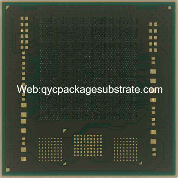
FCBGA Packaging Substrate
FCBGA Packaging Substrate manufacturer. the Package Substrate will be made with Showa Denko and Ajinomoto High speed materials.or other types high speed materials and high frequency materials.
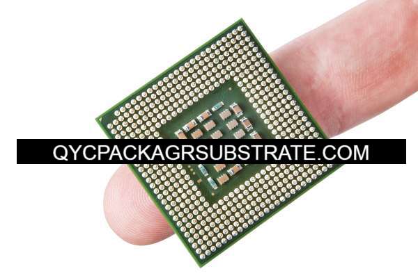
FCBGA, or Flip-Chip Ball Grid Array, Package Substrate refers to a type of substrate used in semiconductor packaging, particularly in the assembly of integrated circuits (ICs) and other electronic components. The term “Flip-Chip” indicates a specific method of connecting the silicon die (chip) to the substrate.
In the FCBGA configuration, the silicon die is flipped upside down, and its active surface, which contains the electrical connections, is directly attached to the package substrate. This is in contrast to traditional packaging methods where the connections are made on the face of the die. The connections are typically made using solder bumps or balls, forming a grid array that provides electrical connections between the die and the substrate.
The package substrate in FCBGA serves as a support structure for the semiconductor device and facilitates the electrical connections between the die and the external circuitry. It is a critical component in the overall reliability and performance of the integrated circuit. The design and materials used in FCBGA package substrates vary based on the specific application and performance requirements of the semiconductor device. This packaging technology is commonly used in applications where space efficiency, thermal management, and high-speed electrical performance are crucial considerations, such as in microprocessors and other high-performance electronic devices.
What Defines FCBGA Package Substrate in PCB Engineering?
FCBGA Package Substrate in PCB engineering is defined by its distinctive characteristics and functionalities, setting it apart in the intricate landscape of electronic design. Let’s explore the fundamental aspects that make FCBGA a pivotal component in modern electronics:
-
Flip-Chip Configuration:
-
- FCBGA is characterized by a flip-chip configuration where the silicon die is inverted and its active surface, containing electrical connections, is directly attached to the package substrate. This flip-chip design enhances electrical performance and thermal management.
-
Grid Array Connections:
-
- The electrical connections between the silicon die and the substrate are established through a grid array of solder bumps or balls. This grid array provides a dense and reliable network of connections, crucial for high-speed and efficient electronic performance.
-
Space Efficiency:
-
- FCBGA excels in space efficiency, making it suitable for applications where compact design is essential. The flip-chip arrangement and grid array configuration contribute to a more compact and streamlined overall package.
-
Thermal Management:
-
- The flip-chip design allows for efficient heat dissipation, making FCBGA well-suited for high-performance applications. Improved thermal management is vital for maintaining the reliability and longevity of electronic components.
- Versatility in Applications:
-
- FCBGA finds applications in a diverse range of electronic devices, particularly those demanding high performance and reliability. From microprocessors to advanced electronic components, FCBGA’s versatility makes it a go-to choice in various industries.
- Manufacturing Technologies:
- The manufacturing technologies associated with FCBGA include advanced processes such as Improved HDI fabrication and Improved Semi-Additive methods. These technologies contribute to the precision and quality of FCBGA package substrates.
In conclusion, FCBGA Package Substrate stands out in PCB engineering due to its innovative design, space efficiency, thermal management capabilities, and suitability for high-speed applications. Understanding these fundamental aspects is essential for engineers and designers navigating the dynamic landscape of modern electronic design.
What Functions Does FCBGA Packaging Substrate Serve?
FCBGA Package Substrate serves a multitude of functions at the core of its design. From structural support to facilitating electrical connections, the key roles that FCBGA plays in enhancing the performance and reliability of electronic components are pivotal:
-
Structural Support:
-
- FCBGA acts as a robust structural support for the semiconductor device. Its design provides stability and protection to the delicate silicon die, safeguarding it against physical stresses and environmental factors.
-
Electrical Connections:
-
- One of the primary functions of FCBGA is to establish electrical connections between the silicon die and the external circuitry. The flip-chip configuration, with solder bumps or balls forming a grid array, ensures efficient and reliable electrical pathways.
-
Heat Dissipation:
-
- FCBGA facilitates effective heat dissipation from the silicon die. The flip-chip design allows for improved thermal management, crucial for preventing overheating and maintaining optimal operating temperatures of electronic components.
-
Space Efficiency:
-
- By adopting a flip-chip arrangement, FCBGA contributes to space efficiency. This is particularly important in modern electronic devices where miniaturization is a key factor, allowing for compact designs without compromising performance.
-
Enhanced Signal Integrity:
-
- The design of FCBGA contributes to enhanced signal integrity. By minimizing the length of electrical pathways, it reduces signal delays and improves the overall speed and reliability of electronic communication within the device.
-
Reliability in High-Speed Applications:
-
- FCBGA is well-suited for high-speed applications due to its efficient electrical connections and thermal management. This makes it a reliable choice for electronic components operating in environments where rapid data transmission and processing are essential.
-
Versatility in Applications:
-
- FCBGA’s functionality extends across a wide range of applications, from microprocessors to high-performance electronic components. Its versatility allows it to meet the demands of various industries seeking both reliability and high functionality.
-
Advanced Manufacturing Compatibility:
- FCBGA’s design and functions are compatible with advanced manufacturing technologies such as Improved HDI fabrication and Improved Semi-Additive methods, ensuring precision and quality in the production process.
In summary, FCBGA Package Substrate serves as a multifunctional component that not only provides structural support and facilitates electrical connections but also contributes to heat dissipation, space efficiency, signal integrity, and reliability in high-speed applications. Understanding and leveraging these functions are crucial for optimizing the performance of electronic components in modern PCB engineering.
What Are the Different Types of FCBGA Packaging Substrate?
Dive into the diverse world of FCBGA variants. How can we categorize and understand these substrates based on materials, manufacturing technologies, and specific applications in the market?
-
Material Types:
-
- Organic Substrate:Most FCBGA package substrates predominantly employ organic materials, commonly crafted from substances like epoxy resin reinforced with glass fibers or polyimide.
- Inorganic Substrate: In high-performance scenarios, certain applications opt for inorganic substrates, including materials like silicon nitride, aluminum nitride, or alumina.
-
Manufacturing Technologies:
-
- Traditional Manufacturing Technology: FCBGA substrates using traditional manufacturing methods follow standard printed circuit board (PCB) manufacturing processes, including copper foil etching, lamination, drilling, etc.
- Advanced Manufacturing Technology: Advanced manufacturing technologies, such as Improved High-Density Interconnect (HDI) fabrication, offer higher circuit density and performance through more precise process steps.
-
Application Fields:
-
- General Electronics: Most types of FCBGA find widespread application in general electronic devices, such as computers, smartphones, and consumer electronics.
- High-Performance Computing: Specialized FCBGA designs may be employed in high-performance computing to meet requirements for high density, speed, and low signal delay.
- Radio Frequency (RF) Applications: Specific FCBGA types may be designed for RF applications, offering superior electrical performance and impedance control.
-
Packaging Forms:
-
- Ball Array Spacing: FCBGA can be categorized into standard and high-density packaging based on the spacing of the ball array to meet different packaging needs.
- Package Size: Smaller-sized FCBGA may be used in thin and light electronic devices, while larger packages are suitable for applications demanding higher performance.
-
Performance Levels:
- Commercial Grade: Targeted at the consumer market, suitable for general consumer electronics.
- Industrial and Military Grade: Tailored for industrial and military applications, demanding higher reliability, durability, and stability.
By categorizing along these dimensions, we can gain a more comprehensive understanding of the different types of FCBGA package substrates and their applications across diverse industry sectors. This aids in selecting the most suitable FCBGA type for specific requirements.
How Does FCBGA Packaging Substrate Differ from PCB?
Distinguishing FCBGA Package Substrate from traditional PCBs is essential for comprehending its role. Through comparisons with PWBs, standard PCBs, motherboards, and advanced technologies like Substrate-like PCB (SLP) and HDI substrate, what unique characteristics does FCBGA bring to the table?
-
Flip-Chip Configuration:
-
- FCBGA employs a flip-chip configuration, where the silicon die is inverted and directly connected to the substrate, enhancing electrical performance compared to traditional PCBs.
-
Grid Array Connections:
-
- FCBGA utilizes a grid array of solder bumps or balls for electrical connections, providing a dense and reliable network, in contrast to the surface-mounted components on standard PCBs.
-
Enhanced Thermal Management:
-
- The flip-chip design of FCBGA facilitates improved heat dissipation, critical for high-performance applications, whereas traditional PCBs may rely on heatsinks or other mechanisms.
-
Compact Design:
-
- FCBGA’s compact design, enabled by the flip-chip arrangement, is advantageous for miniaturized electronic devices, unlike standard PCBs that may have larger footprints.
-
High-Speed Signal Integrity:
-
- FCBGA, with its minimized electrical pathways, enhances signal integrity, reducing delays and ensuring high-speed performance, a feature not as pronounced in conventional PCBs.
-
Application-Specific Designs:
-
- FCBGA is often tailored for specific applications, providing optimized solutions for high-performance computing, telecommunications, and other advanced electronic systems.
- Advanced Manufacturing Techniques:
-
- The production of FCBGA involves advanced manufacturing technologies such as Improved HDI fabrication, contributing to higher precision and reliability compared to standard PCB manufacturing.
-
Versatility in Component Integration:
-
- Unlike standard PCBs, FCBGA allows for the integration of a large number of pins and connections in a relatively small space, making it suitable for complex integrated circuits and microprocessors.
-
Reliability in High-Density Layouts:
- FCBGA excels in high-density layouts, ensuring reliability in densely populated electronic components, a characteristic that may be challenging to achieve with traditional PCBs.
In conclusion, FCBGA Package Substrate stands out by offering advanced electrical and thermal characteristics, compact designs, and high-speed signal integrity, making it a preferred choice for various high-performance electronic applications compared to traditional PCBs.
What Constitutes the Main Structure and Production Technologies of FCBGA Package Substrate?
Delve deeper into the intricate structure of FCBGA Package Substrate. Explore the core elements that define its functionality and manufacturing technologies such as Improved HDI fabrication and the cutting-edge Improved Semi-Additive method.
Main Structure of FCBGA Package Substrate:
The main structure of FCBGA comprises several key elements. The flip-chip configuration places the silicon die upside down, and a grid array of solder bumps connects it to the substrate. This structure provides a foundation for efficient electrical connections and thermal dissipation.
Core Elements Defining Functionality:
Flip-Chip Arrangement: The inverted placement of the silicon die allows for direct electrical connections to the substrate, optimizing signal pathways and reducing signal delays.
Solder Bump Grid Array: The use of a grid array formed by solder bumps ensures a high-density and reliable network of electrical connections, contributing to the overall functionality.
Manufacturing Technologies:
Improved HDI Fabrication (High-Density Interconnect): FCBGA benefits from Improved HDI fabrication, a manufacturing technique that enhances circuit density by using finer lines and spaces. This technology allows for more intricate and compact designs, crucial for miniaturized electronic devices.
Improved Semi-Additive Method: This cutting-edge manufacturing method involves selectively adding material to create circuit patterns, providing a higher level of precision compared to traditional subtractive methods. The Improved Semi-Additive method contributes to the intricate design and reliability of FCBGA package substrates.
Role of Improved HDI Fabrication:
Improved HDI fabrication enhances the overall performance of FCBGA by enabling the creation of finer and more densely packed circuitry. This is particularly advantageous in meeting the demands of high-speed electronic applications.
Cutting-Edge Improved Semi-Additive Method:
The Improved Semi-Additive method allows for precise and controlled addition of material during the manufacturing process, resulting in highly defined circuit patterns. This method is pivotal in achieving the intricate layouts required for advanced electronic components.
Advantages of Advanced Manufacturing:
The integration of Improved HDI fabrication and the Improved Semi-Additive method brings advantages such as increased precision, reduced signal interference, and improved reliability, ensuring that FCBGA package substrates meet the stringent requirements of modern electronic designs.
In summary, the main structure of FCBGA Package Substrate revolves around the flip-chip configuration and solder bump grid array. Its functionality is defined by core elements such as the flip-chip arrangement and manufacturing technologies like Improved HDI fabrication and the state-of-the-art Improved Semi-Additive method. These advanced manufacturing techniques contribute to the intricate design and superior performance of FCBGA in the realm of electronic packaging.
What Are Common Questions about FCBGA Package Substrate?
1. What does FCBGA stand for, and what is its significance in electronic packaging?
FCBGA stands for Flip-Chip Ball Grid Array. It is a semiconductor packaging technology where the silicon die is inverted and electrically connected to the substrate. Its significance lies in its ability to enhance electrical performance, thermal management, and space efficiency in electronic devices.
2. How does FCBGA differ from traditional PCBs?
FCBGA differs from traditional Printed Circuit Boards (PCBs) in its flip-chip configuration, grid array connections, and enhanced thermal management. Unlike standard PCBs, FCBGA’s design allows for compact layouts, improved signal integrity, and efficient heat dissipation.
3. What are the key applications of FCBGA?
FCBGA finds applications in high-performance electronic devices such as microprocessors, high-speed computing systems, telecommunications equipment, and other applications demanding compact design and reliability.
4. What role does the flip-chip configuration play in FCBGA?
The flip-chip configuration involves inverting the silicon die, allowing direct electrical connections to the substrate. This design enhances signal pathways, reduces delays, and improves thermal management.
5. Can you explain the significance of Improved HDI fabrication in FCBGA manufacturing?
Improved High-Density Interconnect (HDI) fabrication is crucial in FCBGA manufacturing. It enables higher circuit density through finer lines and spaces, contributing to more intricate and compact designs, especially beneficial for miniaturized electronic devices.
6. How does FCBGA contribute to high-speed electronic applications?
FCBGA enhances signal integrity and reduces electrical noise, making it suitable for high-speed electronic applications. The compact design, flip-chip configuration, and efficient electrical connections contribute to its high-speed performance.
7. Are there specific industries where FCBGA is commonly used?
FCBGA is commonly used in industries such as telecommunications, computing, aerospace, and other sectors requiring high-performance and reliable electronic components.
8. What advantages do FCBGA package substrates offer in terms of space efficiency?
FCBGA’s compact design and efficient use of space make it suitable for applications where space efficiency is critical, such as in mobile devices, where minimizing the footprint is essential.
9. How does FCBGA contribute to heat dissipation in electronic devices?
The flip-chip design of FCBGA allows for effective heat dissipation from the silicon die, contributing to thermal management and preventing overheating in high-performance electronic devices.
10. Are there variations in FCBGA designs for different applications?
Yes, FCBGA designs may vary based on specific applications and performance requirements. Variations include different ball array spacing, materials used, and design considerations tailored to the intended use.
Why is FCBGA Package Substrate a Linchpin in PCB Engineering?
In conclusion, explore the significance of FCBGA Package Substrate as a linchpin in the evolution of PCB engineering. This article serves as a guide, emphasizing the importance of delving into the nuances of FCBGA for engineers, designers, and enthusiasts navigating the ever-evolving landscape of electronic design.
In the dynamic field of PCB engineering, the FCBGA Package Substrate stands out as a linchpin, playing a pivotal role in shaping the trajectory of electronic design. Its significance can be attributed to several key factors:
-
Enhanced Electrical Performance:
-
- FCBGA’s flip-chip configuration and grid array connections contribute to improved electrical performance, offering faster signal transmission and reduced signal delays. This is crucial in high-speed electronic applications, making FCBGA a linchpin for achieving optimal performance.
-
Efficient Thermal Management:
-
- The flip-chip design of FCBGA facilitates efficient heat dissipation from the silicon die, preventing overheating and ensuring the reliability of electronic components. This is especially important in high-performance computing and other demanding applications.
-
Space-Efficient Design:
-
- FCBGA’s compact design allows for the integration of a large number of pins and connections in a relatively small space. This space efficiency is essential in the era of miniaturized electronic devices and contributes to the linchpin status of FCBGA in modern PCB engineering.
-
Advanced Manufacturing Compatibility:
-
- FCBGA’s compatibility with advanced manufacturing technologies, such as Improved HDI fabrication and the Improved Semi-Additive method, positions it as a linchpin in embracing cutting-edge processes. This compatibility ensures precision and reliability in the production of electronic components.
-
Application Versatility:
-
- FCBGA finds applications across diverse industries, from consumer electronics to telecommunications and high-performance computing. Its versatility in addressing the specific needs of various applications makes it a linchpin for engineers seeking adaptable solutions.
-
Evolutionary Impact on PCB Designs:
- The adoption of FCBGA has influenced the evolution of PCB designs, pushing the boundaries of what is achievable in terms of performance, miniaturization, and reliability. Engineers and designers increasingly rely on FCBGA to meet the growing demands of modern electronic systems.
In conclusion, FCBGA Package Substrate serves as a linchpin in PCB engineering due to its contributions to enhanced electrical performance, efficient thermal management, space-efficient design, compatibility with advanced manufacturing, application versatility, and its impact on the evolutionary trajectory of PCB designs. Engineers, designers, and enthusiasts are encouraged to delve into the intricacies of FCBGA, recognizing it as a cornerstone in the ever-evolving landscape of electronic design.