
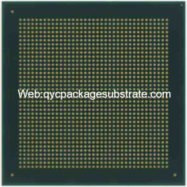
What is FCBGA Packaging?
We are a professional FCBGA Packaging substrate provider, we mainly produce ultra-small bump pitch with 100um, the microtrace and spacing are 9um/9um. when we make this microtrace FC BGA substrates. we have to use the Showa Denko and Ajinomoto series materials. or other high quality base materials.
FCBGA stands for Flip-Chip Ball Grid Array, and it is a type of chip packaging technology used in the manufacturing of integrated circuits. FCBGA packaging is characterized by a ball grid array (BGA) arrangement and the use of a flip-chip design. Let’s break down the key elements that define FCBGA packaging as an advanced chip packaging technology:
Flip-Chip Design:
In a flip-chip design, the active side of the semiconductor die is flipped and attached directly to the substrate or carrier. This is different from traditional packaging methods where the chip is wire-bonded to the package.
The flip-chip design offers advantages such as shorter interconnection lengths, reduced parasitic capacitance and inductance, and improved thermal performance.
Ball Grid Array (BGA):
BGA is a type of surface-mount packaging used for integrated circuits. Instead of traditional pins, the package has an array of solder balls on the bottom side.
These solder balls are used for electrical connections and mechanical attachment to the PCB (Printed Circuit Board). BGA provides better thermal and electrical performance compared to some other packaging methods.
Tiny Pitch Spacing:
Pitch refers to the distance between the centers of adjacent solder balls in the grid array. FCBGA packaging is known for having a very small pitch, meaning that the solder balls are closely spaced.
Reduced pitch spacing is essential in accommodating a greater number of interconnections, facilitating increased input/output (I/O) connections within a confined space. This becomes particularly critical for contemporary integrated circuits characterized by a multitude of transistors and intricate functionalities.
Advanced Chip Packaging Technology:
FCBGA is considered an advanced chip packaging technology due to its ability to meet the requirements of high-performance and compact electronic devices.
The combination of flip-chip design, BGA, and tiny pitch spacing contributes to improved electrical performance, thermal management, and overall miniaturization of electronic components.
In summary, FCBGA packaging is an advanced chip packaging technology that incorporates a flip-chip design, a ball grid array, and tiny pitch spacing. These features collectively contribute to enhanced performance, compactness, and reliability in integrated circuits, making it a suitable choice for various electronic applications.
What Functions Does FCBGA Packaging Serve?
FCBGA (Flip-Chip Ball Grid Array) packaging serves several critical functions in electronic devices, playing a pivotal role in connection reliability and heat dissipation. Here’s an overview of the functions of FCBGA packaging:
Connection Density:
FCBGA packaging allows for a high density of interconnections due to its tiny pitch spacing and ball grid array design. This is crucial for modern integrated circuits that have a large number of components, as it enables more connections in a limited space.
Electrical Interconnections:
The solder balls in the ball grid array serve as electrical connections between the integrated circuit (IC) and the printed circuit board (PCB). The flip-chip design contributes to shorter interconnection lengths, reducing signal propagation delays and improving overall electrical performance.
Heat Dissipation:
The flip-chip design of FCBGA packaging plays a significant role in heat dissipation. The direct attachment of the active side of the semiconductor die to the substrate enhances thermal conductivity. This is crucial for managing the heat generated by the electronic components during operation.
Improved Signal Integrity:
FCBGA packaging helps maintain signal integrity by minimizing the length of electrical paths and reducing parasitic capacitance and inductance. This contributes to better performance in terms of signal transmission and reception.
Mechanical Stability:
The ball grid array provides mechanical stability by evenly distributing the mechanical stress across the solder balls. This contributes to the overall robustness of the packaged IC, making it more resistant to mechanical shocks and vibrations.
Miniaturization:
FCBGA packaging supports the trend of miniaturization in electronic devices. The combination of a flip-chip design and tiny pitch spacing allows manufacturers to produce smaller and more compact ICs, which is crucial for applications where space is at a premium.
Reliability:
The design features of FCBGA packaging contribute to the overall reliability of electronic devices. The direct attachment of the flip-chip design and the robustness of the ball grid array enhance the durability and longevity of the integrated circuits.
In summary, FCBGA packaging serves critical functions in electronic devices, including providing high connection density, facilitating electrical interconnections, aiding in efficient heat dissipation, improving signal integrity, ensuring mechanical stability, supporting miniaturization, and enhancing overall reliability. These functions collectively contribute to the optimal performance and longevity of electronic devices.
What Constitutes the Structure and Types of FCBGA Packaging?
The structure of FCBGA (Flip-Chip Ball Grid Array) packaging involves several key elements, and there are different types tailored to meet various application requirements. Here’s an overview of the structure and types:
Structure of FCBGA Packaging:
Semiconductor Die:
The central component is the semiconductor die, which contains the actual electronic circuitry.
Flip-Chip Configuration:
The die is flipped upside down, and its active side is directly bonded to the package substrate using solder bumps or C4 (controlled collapse chip connection). This flip-chip configuration reduces the distance between the die and the substrate, enhancing electrical performance.
Package Substrate:
The package substrate serves as the foundation for the semiconductor die and provides a platform for the flip-chip bonding. It is typically made of materials like fiberglass-reinforced epoxy (FR-4) or other high-performance materials.
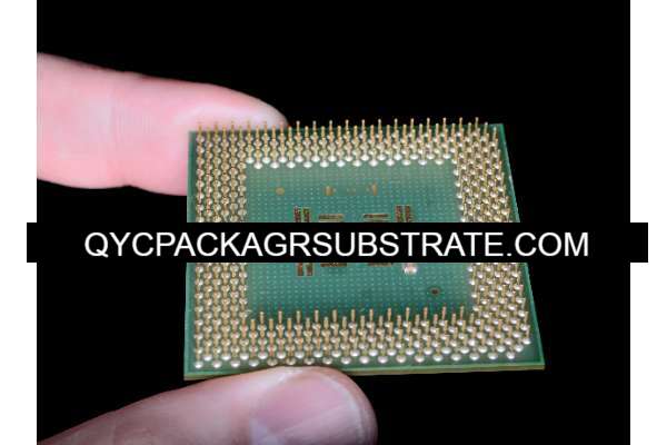
Solder Balls (Bumps):
Tiny solder balls are deposited on the active side of the semiconductor die. These solder balls serve as both the electrical and mechanical connections between the die and the package substrate. They form the external connections to the circuit board.
Ball Grid Array (BGA):
The bottom side of the package features an array of solder balls in a grid pattern. These balls serve as the external connections to the circuit board when the FCBGA package is mounted.
Underfill Material:
To enhance the mechanical stability and reliability of the package, an underfill material is often used to fill the space between the semiconductor die and the package substrate.
Types of FCBGA Packaging:
Standard FCBGA:
This is the basic form of FCBGA packaging, suitable for a wide range of applications. It offers the advantages of a flip-chip design, shorter interconnects, and improved thermal performance.
Enhanced FCBGA:
Enhanced FCBGA packages may incorporate additional features or materials to further improve performance, such as advanced thermal management solutions, specialized coatings, or enhancements for specific industry requirements.
Multi-Chip Modules (MCM):
Some FCBGA packages are designed to accommodate multiple semiconductor dies within the same package. This is known as a multi-chip module, where different dies with complementary functions are integrated into a single package.
Application-Specific FCBGA:
FCBGA packaging can be tailored for specific applications, such as high-performance computing, graphics processing, or communication applications. These versions may have design optimizations to meet the unique demands of each application.
Stacked FCBGA:
In stacked FCBGA configurations, multiple semiconductor dies are vertically stacked within the same package. This allows for increased functionality and component density in a compact form factor.
Each type of FCBGA packaging is designed to address specific requirements, such as performance, thermal management, and integration capabilities, making them versatile for a wide range of semiconductor applications.
How Does FCBGA Packaging Relate to FCBGA PCBs?
FCBGA (Flip-Chip Ball Grid Array) packaging and FCBGA PCB (Printed Circuit Board) are closely related components within the broader context of electronic systems. The relationship between FCBGA packaging and FCBGA PCB significantly impacts the overall performance of electronic systems. Here’s how they are interconnected:
Design Compatibility:
FCBGA packaging and FCBGA PCBs are designed to be compatible with each other. The layout of the solder balls on the FCBGA package corresponds to the arrangement of the pads on the FCBGA PCB, ensuring proper alignment and connectivity.
Electrical Connectivity:
The solder balls on the FCBGA package serve as electrical connections to the FCBGA PCB. These connections are vital for the transfer of signals and power between the integrated circuit (IC) and the PCB. The close alignment and connectivity contribute to efficient electrical performance.
Signal Integrity:
The design synergy between FCBGA packaging and FCBGA PCB helps maintain signal integrity. The short interconnection lengths and carefully aligned connections minimize signal distortion, ensuring that data and signals are transmitted accurately and reliably.
Thermal Management:
The direct attachment of the flip-chip design in FCBGA packaging to the FCBGA PCB facilitates effective heat dissipation. The PCB acts as a heat sink, helping to transfer and dissipate heat away from the IC. This is crucial for preventing overheating and maintaining the electronic components’ operational reliability.
Mechanical Stability:
The mechanical stability provided by the FCBGA package, with its ball grid array, is complemented by the mechanical support offered by the FCBGA PCB. Together, they enhance the overall mechanical resilience of the integrated system, bolstering its resistance to physical stresses and environmental influences.
Manufacturability:
FCBGA packaging and FCBGA PCBs are crafted with manufacturability as a central consideration. The alignment of solder balls with PCB pads streamlines the assembly process, improving the robustness of manufacturing and diminishing the probability of defects.
Form Factor and Size:
The combination of FCBGA packaging and FCBGA PCBs supports a compact form factor. This is especially important in modern electronic devices where space is a premium. The smaller footprint contributes to the miniaturization of electronic systems.
Overall System Performance:
The close relationship between FCBGA packaging and FCBGA PCB directly influences the overall performance of electronic systems. Efficient electrical connectivity, thermal management, signal integrity, and mechanical stability contribute to a reliable and high-performing electronic system.
In summary, the relationship between FCBGA packaging and FCBGA PCBs is integral to the successful operation of electronic systems. Their compatibility, alignment, and collaborative design significantly impact the overall performance, reliability, and manufacturability of electronic devices.
How Does FCBGA Packaging Compare with Traditional PCBs?
FCBGA (Flip-Chip Ball Grid Array) packaging and traditional PCBs (Printed Circuit Boards) serve distinct roles in electronic systems, especially in the context of motherboard design. Here are key differences between FCBGA packaging and traditional PCBs:
Packaging Technology:
FCBGA is a specific packaging technology used for individual integrated circuits, focusing on the arrangement of solder balls for electrical connections. Traditional PCBs, on the other hand, refer to the entire board that hosts various components, including integrated circuits, resistors, capacitors, etc.
Chip Attachment:
FCBGA utilizes a flip-chip design where the active side of the semiconductor die is directly attached to the substrate using solder bumps. Traditional PCBs typically involve components being attached to the board via methods like through-hole or surface-mount technology, using leads or pads.
Interconnection Density:
FCBGA is known for its tiny pitch spacing, enabling a high density of interconnections. This is crucial for modern integrated circuits with numerous transistors. Traditional PCBs may have larger spacing, limiting the number of connections in a given area.
Miniaturization:
FCBGA packaging supports miniaturization due to its compact design, enabling the creation of smaller and more densely packed integrated circuits. Traditional PCBs may be larger and less conducive to achieving the same level of miniaturization.
Heat Dissipation:
FCBGA packaging, with its flip-chip design, allows for efficient heat dissipation by directly attaching the semiconductor die to the substrate. Traditional PCBs manage heat through methods such as heat sinks, thermal vias, and copper planes.
Specialized Applications:
FCBGA packaging is commonly employed in high-performance integrated circuits, notably in CPUs and GPUs. In contrast, traditional PCBs find applications across a diverse range of electronic components and systems, catering to simpler and less heat-intensive functionalities.
Complexity and Cost:
FCBGA packaging tends to be more complex and can be costlier due to its advanced technology and the precision required for manufacturing. Traditional PCBs vary widely in complexity and cost, depending on the application and specific design requirements.
Motherboard Design:
In the context of motherboard design, FCBGA packaging is typically used for critical components like the CPU and GPU. Traditional PCBs make up the entire motherboard, providing the platform for various components, connectors, and expansion slots.
In summary, FCBGA packaging and traditional PCBs represent different aspects of electronic system design. FCBGA focuses on the packaging and interconnection of individual integrated circuits, especially those with high-performance requirements, while traditional PCBs form the foundation for entire electronic systems, including motherboards, with a broader range of applications and components.
What Comprises the Production Technology and Structure of FCBGA Packaging?
The production technology and structure of FCBGA (Flip-Chip Ball Grid Array) packaging involve several key structural features, including fine-pitch pins and ball arrays. These components are manufactured using advanced High-Density Interconnect (HDI) techniques and semi-additive methods. Here are the main aspects:
Flip-Chip Design:
FCBGA packaging employs a flip-chip design where the active side of the semiconductor die is flipped and directly connected to the substrate. This design reduces signal propagation delays and enhances electrical performance.
Fine-Pitch Pins:
Fine-pitch pins refer to the closely spaced pins or solder balls on the bottom of the FCBGA package. The small pitch allows for a higher density of connections, accommodating the increasing number of I/Os in modern integrated circuits.
Ball Arrays (Ball Grid Array):
The solder balls on the bottom of the FCBGA package form a Ball Grid Array (BGA). This array provides electrical connections and mechanical support when the package is mounted on a PCB.
High-Density Interconnect (HDI) Techniques:
HDI techniques involve creating intricate interconnections between the various layers of the FCBGA package. This is achieved using advanced manufacturing processes that allow for high density and precision in routing signals between different components.
Semi-Additive Methods:
Semi-additive methods involve selectively adding material to build up the necessary features on the substrate. In FCBGA packaging, semi-additive methods are often used to create fine traces and pads, contributing to the compact design and improved performance.
Die Attach and Underfill:
The semiconductor die is attached to the substrate using die attach materials, ensuring a secure and reliable connection. Underfill materials are often applied to enhance the mechanical strength of the joint and provide additional protection against thermal and mechanical stresses.
Build-Up Layers:
FCBGA packages typically have multiple build-up layers. These layers include the substrate, dielectric layers, and conductive layers, allowing for the creation of complex and compact circuitry.
Advanced Materials:
FCBGA packaging often utilizes advanced materials such as low-dielectric constant (low-k) materials to reduce signal propagation delays and improve overall electrical performance. These materials also contribute to better thermal management.
Manufacturing Process:
The manufacturing process for FCBGA packaging involves a combination of photolithography, plating, and etching steps. These steps are repeated to create the multiple layers and features required for the complex interconnections.
Quality Control and Inspection:
Ensuring the reliability and performance of FCBGA packaging is contingent upon rigorous quality control measures, involving comprehensive inspection and testing. Utilizing advanced inspection techniques like X-ray imaging becomes essential to identify and address any defects or irregularities in the packaging.
In summary, FCBGA packaging is characterized by its flip-chip design, fine-pitch pins, ball arrays, and the use of advanced manufacturing techniques such as HDI and semi-additive methods. These features collectively contribute to the high performance, reliability, and compact design of FCBGA packages, making them suitable for applications in high-performance integrated circuits like CPUs and GPUs.
What Are the FAQs About FCBGA Packaging?
1. What is FCBGA packaging?
FCBGA (Flip-Chip Ball Grid Array) packaging is an advanced technology used in semiconductor packaging. It involves a flip-chip design where the active side of the semiconductor die is directly connected to the substrate using solder balls.
2. What distinguishes FCBGA packaging from other packaging types?
FCBGA stands out for its flip-chip design, enabling shorter interconnection lengths, higher connection density, and efficient heat dissipation. These features make it suitable for high-performance integrated circuits.
3. In what applications is FCBGA packaging commonly used?
FCBGA packaging is frequently employed in high-performance integrated circuits found in CPUs, GPUs, and other applications requiring compact design, high connection density, and efficient heat management.
4. How does FCBGA packaging contribute to miniaturization?
The flip-chip design and tiny pitch spacing of FCBGA packaging allow for a smaller footprint, supporting the trend of miniaturization in electronic devices.
5. What role does FCBGA packaging play in heat dissipation?
The direct attachment of the flip-chip design to the substrate enhances thermal conductivity, facilitating effective heat dissipation. This is crucial for managing the heat generated by high-performance electronic components.
6. How are defects in FCBGA packaging detected during manufacturing?
Advanced inspection techniques, including X-ray imaging, are often employed to detect defects or irregularities in FCBGA packaging during the manufacturing process. Thorough quality control measures ensure reliability.
7. What are the advantages of FCBGA packaging in terms of signal integrity?
FCBGA packaging minimizes signal propagation delays by reducing interconnection lengths. This contributes to improved signal integrity, crucial for the reliable transmission of data and signals.
8. Can FCBGA packaging be used in a wide range of electronic devices?
While FCBGA is commonly used in high-performance applications like CPUs and GPUs, its versatility allows it to be applied in various electronic devices requiring compact design and efficient interconnections.
9. How is the alignment of solder balls with PCB pads achieved in FCBGA packaging?
Precision manufacturing techniques, such as High-Density Interconnect (HDI) and semi-additive methods, ensure the accurate alignment of solder balls with PCB pads, simplifying the assembly process.
10. What considerations are important for the reliability of FCBGA packaging?
Thorough quality control, proper material selection, and adherence to manufacturing standards are critical for ensuring the reliability of FCBGA packaging, especially in applications with high-performance requirements.
These FAQs aim to provide readers with essential insights into FCBGA packaging, addressing common questions and helping them better understand the features, applications, and advantages of this advanced packaging technology.
What Insights Does FCBGA Packaging Provide for the Future of High-Performance Electro nic Devices?
Miniaturization and Compact Design:
FCBGA packaging’s role in enabling miniaturization is crucial for the development of smaller and more compact high-performance electronic devices. As technology advances, the demand for smaller form factors continues to grow, making FCBGA a key player in this trend.
Increased Connection Density:
The tiny pitch spacing and fine-pitch pins of FCBGA packaging allow for a higher density of interconnections. This is essential as electronic devices become more complex, requiring a greater number of connections for enhanced functionality. FCBGA supports the evolving needs of high-performance applications.
Improved Thermal Management:
FCBGA’s efficient heat dissipation properties contribute to better thermal management in high-performance devices. As electronic components become more powerful, managing heat becomes increasingly critical to prevent overheating and ensure reliable operation. FCBGA’s design addresses this challenge.
Enhanced Signal Integrity:
The design of FCBGA packaging minimizes signal propagation delays, contributing to enhanced signal integrity. This is crucial for high-performance electronic devices where accurate and fast data transmission is essential.
Versatility Across Applications:
FCBGA packaging is adaptable and finds application in a diverse range of high-performance electronic devices. From CPUs and GPUs to other advanced integrated circuits, FCBGA’s versatility positions it as a technology capable of meeting the demands of various applications.
Advanced Manufacturing Techniques:
The use of advanced manufacturing techniques, including High-Density Interconnect (HDI) and semi-additive methods, underscores the continuous innovation in FCBGA packaging. These techniques contribute to the precision, reliability, and manufacturability of high-performance devices.
Technological Convergence:
FCBGA packaging plays a role in facilitating technological convergence by providing a platform for integrating diverse functionalities into compact devices. This convergence is evident in devices that combine computing, communication, and sensor technologies.
Proliferation in IoT and Edge Computing:
As the Internet of Things (IoT) and edge computing continue to expand, FCBGA packaging supports the development of devices with high computational power and connectivity in constrained spaces. This is especially relevant in applications where data processing occurs at the edge of the network.
High Reliability for Critical Applications:
FCBGA’s design and manufacturing processes prioritize reliability, making it suitable for critical applications in aerospace, automotive, and medical industries. The technology’s robustness positions it for use in devices where failure is not an option.
Integration with Emerging Technologies:
FCBGA packaging is well-positioned to integrate with emerging technologies such as artificial intelligence, 5G, and quantum computing. Its ability to handle high data throughput and efficient heat dissipation aligns with the demands of these cutting-edge technologies.
In summary, FCBGA packaging provides a foundation for the future of high-performance electronic devices by supporting miniaturization, enhancing connection density, managing heat effectively, ensuring signal integrity, and adapting to a diverse range of applications. As technology evolves, FCBGA is poised to play a central role in shaping the landscape of high-performance electronics.