
What is High-Frequency Package Substrate?
High frequency package substrate supplier. High speed and high frequency material packaging substrate manufacturing. Advanced packaging substrate production process and technology.
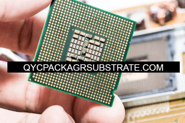
High-Frequency Package Substrate stands out as a specialized foundation for integrating circuits, especially in the microelectronics realm. The “high-frequency” tag indicates its prowess in efficiently handling frequencies in the gigahertz (GHz) range and above.
This substrate takes on the role of a cornerstone, facilitating the mounting and interconnection of diverse electronic components within an integrated circuit package. Its significance lies in delivering electrical connectivity, managing thermal aspects, and offering mechanical support for semiconductor devices.
In the realm of high-frequency applications, prevalent in cutting-edge communication systems, radar setups, and rapid data processing, the substrate’s performance takes center stage. High-frequency signals bring forth distinctive features and challenges, encompassing signal loss, impedance matching intricacies, and the specter of electromagnetic interference. Design and material attributes of the substrate must undergo meticulous optimization to counter these challenges and ensure the integrated circuit’s steadfast operation at high frequencies.
Materials commonly enlisted for high-frequency package substrates include specialized laminates and ceramics flaunting low dielectric constants and controlled impedance traits. These materials play a pivotal role in curbing signal losses and upholding signal integrity within high-frequency environments.
The design and manufacturing processes for these substrates delve into precision engineering, aiming for stringent tolerances to guarantee the desired electrical performance. Engineers and designers immerse themselves in considerations like trace geometry, layer stacking nuances, and overall layout intricacies to fine-tune signal transmission and diminish electromagnetic interference.
In essence, High-Frequency Package Substrate emerges as a linchpin in the packaging of integrated circuits tailored for high-frequency applications. Its role extends beyond mere containment, providing indispensable electrical, thermal, and mechanical support to usher electronic devices into reliable operation within the realms of advanced communication and signal processing systems.
What Functions Does High-Frequency Package Substrate Serve?
High-Frequency Package Substrate is a versatile linchpin in the world of integrated circuits, especially when navigating the complexities of high-frequency domains, typically exceeding the gigahertz (GHz) range. Let’s delve into its diverse functionalities:
Conductor of Electrical Symphony: At its core, the substrate acts as a facilitator for mounting and interconnecting electronic components within an integrated circuit package. It sets the stage for a harmonious flow of electrical signals, ensuring seamless communication and cooperative functionality.
Guardian of Signal Purity: In the intricate dance of high-frequency applications, the substrate is meticulously choreographed to minimize signal losses and impedance dissonance. This dance safeguards the transmission of high-frequency signals, preserving their true essence and preventing distortion.
Heat Choreographer: The dynamic performance of high-frequency operations often raises the temperature. The substrate takes on the role of a choreographer, orchestrating the dissipation of heat away from vital components. This ensures the entire ensemble of semiconductor devices maintains a cool and reliable performance.
Architect of Mechanical Resilience: Beyond its electrical and thermal duties, the substrate serves as an architect of stability. It provides the necessary scaffolding to secure components, offering a robust defense against the rigors of mechanical stress during both handling and operational crescendos.
Material Maestro for High Frequencies: Crafted from materials akin to a virtuoso’s instrument, high-frequency package substrates boast low dielectric constants and controlled impedance. This material composition orchestrates a symphony of mitigated signal loss and preserved signal integrity in the face of high-frequency challenges.
Impedance Harmony Conductor: The substrate’s design harmonizes with impedance matching principles, ensuring a seamless alignment of component and transmission line impedances. This precision orchestration optimizes signal transfer, preventing disruptive reflections that could tarnish the signal’s melody.
EMI (Electromagnetic Interference) Alleviator: High-frequency signals are vulnerable to interference, and the substrate is intricately designed to be an alleviator. Its composition acts as a shield, minimizing the risk of unwanted disruptions or interference, allowing the electronic performance to resonate without discord.
Precision Engineering Artisan: The design and manufacturing processes are a work of precision engineering artistry. Trace geometry, layer stacking, and overall layout are meticulously crafted brushstrokes, fine-tuning the canvas of signal transmission and insulating against external disturbances.
In essence, High-Frequency Package Substrate emerges as a maestro, conducting a symphony of electrical connectivity, signal purity, thermal equilibrium, structural fortitude, and material finesse. Its purposeful design caters to the nuanced challenges presented by high-frequency applications, casting a spotlight on the grand stage of advanced communication systems, radar orchestrations, and high-speed data processing.
What Types of High-Frequency Package Substrate Exist?
Diverse in their capabilities, High-Frequency Package Substrates unfold an assortment of types, each meticulously crafted to tackle specific challenges encountered in various high-frequency applications. Let’s embark on a journey through this spectrum of options:
Rigid-Flex Marvels: Blending the robustness of traditional materials with the flexibility of bendable counterparts, rigid-flex substrates bring versatility to three-dimensional configurations. They shine in scenarios where spatial constraints or intricate form factors take precedence.
Multilayered Wizards: High-frequency multilayered substrates reveal a stacked composition of multiple material layers. This strategic layering not only allows for intricate designs but also plays a pivotal role in achieving controlled impedance, a critical factor for preserving high-frequency signal integrity.
Ceramic Champions: Stepping onto the stage with stellar thermal properties, ceramic substrates exhibit high thermal conductivity. Ideal for applications requiring efficient heat dissipation, ceramics also boast low dielectric constants, contributing to the preservation of signal integrity.
PTFE Prowess: Substrates hewn from polytetrafluoroethylene (PTFE), commonly known as Teflon, carve a niche with their low dielectric constant and minimal loss tangent. PTFE-based substrates excel in minimizing signal loss, making them a preferred choice for high-frequency applications.
Duroid Dynamos: Duroid, a specialized material, finds its place in high-frequency circuit boards. Offering commendable thermal stability and low dielectric loss, Duroid substrates cater to applications demanding consistent electrical performance across varying temperatures.
RF PCB Virtuosos: Designed specifically for radio frequencies, RF PCBs are tailored for optimal signal transmission in wireless communication systems. They carve a unique space in the spectrum of high-frequency substrates.
Metal Core Maestros: With a core of metal, typically aluminum, metal core PCBs stand out for their enhanced thermal conductivity. These substrates take the stage in effectively managing heat in applications with high power and frequencies.
LTCC Innovations: Low-Temperature Co-Fired Ceramic (LTCC) substrates merge ceramics with the capability to integrate passive components within the substrate. This integration prowess proves advantageous in compact high-frequency systems.
Polyimide Pioneers: Offering flexibility, polyimide substrates find their role in applications requiring bendability or conformal designs. They gracefully adapt to the demands of flexible high-frequency circuits.
FR-4 with a High-Frequency Twist: While FR-4 is a familiar substrate, its high-frequency variants boast enhanced properties. Cost-effective and versatile, they find their place in a spectrum of electronic applications.
The selection of a particular high-frequency package substrate hinges on factors such as the targeted frequency range, thermal requisites, form factor considerations, and the overarching performance demands of the application. Engineers deftly navigate this array of substrate options to ensure an optimal match for their high-frequency endeavors.
How Does High-Frequency Package Substrate Differ from Traditional PCB?
Diverging from the well-trodden path of traditional Printed Circuit Boards (PCBs), High-Frequency Package Substrates emerge as bespoke solutions finely tuned for the challenges presented by high-frequency applications. Let’s uncover the distinctive facets that set them apart:
Material Symphony:
High-Frequency Package Substrate: Dance of specialized materials, such as ceramic, PTFE, or Duroid, takes center stage, boasting low dielectric constants. This choreography aims to minimize signal losses and orchestrate controlled impedance, a key melody in high-frequency signals.
Traditional PCB: The familiar hum of FR-4 resonates, a versatile tune but one that may not hit the high notes demanded by the nuances of high-frequency environments.
Dielectric Dynamics:
High-Frequency Package Substrate: Striving for a low dielectric crescendo, these substrates aim to maintain signal speed and prevent distortion, crafting a composition that resonates with the frequencies at play.
Traditional PCB: Dielectric constants in traditional PCBs play a supporting role, not necessarily the lead, in the broader spectrum of applications.
Impedance Improvisation:
High-Frequency Package Substrate: The conductor’s precision in controlling impedance is paramount, fine-tuning the ensemble to match the unique requirements of high-frequency signals and ensuring a harmonious signal integrity.
Traditional PCB: While impedance considerations are present, they may not take the spotlight as they do in the high-frequency arena.
Signal Safari:
High-Frequency Package Substrate: The quest to minimize signal loss and attenuation is an adventurous endeavor, safeguarding the vigor and purity of high-frequency signals as they traverse the circuitry landscape.
Traditional PCB: The consideration of signal loss is a familiar note but may not command the same adventurous spirit as in high-frequency compositions.
Thermal Tactics:
High-Frequency Package Substrate: Battling the thermal tempests, these substrates strategically deploy advanced thermal management features to keep the performance temperature just right in the high-frequency symphony.
Traditional PCB: Thermal considerations persist but may not require the same virtuosity in traditional compositions.
Layering Legato:
High-Frequency Package Substrate: Layers weave a sonnet of intricacy, with precise trace geometries composing an opus to optimize signal paths and minimize the discord of electromagnetic interference.
Traditional PCB: While complexity exists, the layering may not be as nuanced in traditional compositions.
Flexibility Flourish:
High-Frequency Package Substrate: Flexibility takes a bow, especially in applications where the design demands a ballet of conformal or bendable movements.
Traditional PCB: While the dance of flexible PCBs is known, it may not sway to the same rhythm in the conventional ballroom.
In essence, High-Frequency Package Substrates compose a specialized symphony, harmonizing through unique materials, impedance mastery, and a keen ear for signal integrity, orchestrating a melody finely attuned to the intricacies of high-frequency applications. Traditional PCBs, with their versatile repertoire, may find themselves in a different ensemble, playing to a broader audience.
What Constitutes the Main Structure and Production Technologies?
Crafting the main structure of High-Frequency Package Substrates involves a symphony of materials and cutting-edge production technologies, meticulously orchestrated to meet the demands of high-frequency applications. Let’s delve into the composition and manufacturing intricacies:
Main Structure:
Foundation Materials:
High-Frequency Alchemy: The journey begins with the selection of specialized materials like ceramics, PTFE, or Duroid. These materials, chosen for their low dielectric constants, lay the foundation for optimal signal performance.
Layered Brilliance:
Strategic Layering: The substrate unfolds in multiple layers, each strategically designed to achieve controlled impedance, foster precise signal paths, and provide a robust mechanical structure.
Trace Artistry:
Precision in Lines: Conductive traces dance across the substrate with precision. Engineered for minimal signal losses and impedance harmony, these traces waltz in intricate geometries.
Grounded Realms:
Ground and Power Poise: Dedicated ground and power planes enter the scene, enhancing signal integrity. Isolation and proper grounding become the pillars of stability.
Dielectric Harmony:
Low-Dielectric Serenade: Between the conductive traces, dielectric layers embrace materials with low dielectric constants. This serenade maintains signal speed and orchestrates a harmonious frequency response.
Surface Elegance:
Finishing Flourish: Surface finishes, often adorned in gold or immersion silver, add an elegant touch. Ensuring conductivity and preventing oxidation, they contribute to the substrate’s overall performance.
Production Technologies:
Material Prelude:
Art of Selection: The production overture commences with the careful selection of materials tailored to the specific needs of high-frequency applications.
Lamination Choreography: For multilayer substrates, layers engage in a dance of lamination, merging seamlessly under heat and pressure.
Trace Etching Sonata:
Precision Photoetching: The substrate comes to life through precision photoetching, a chemical dance that sculpts the intricate conductive traces with accuracy.
Drilling Crescendo:
Micro-Drilling Cadence: Small-diameter drills engage in a cadence of drilling, creating vias and openings to connect different layers and elements.
Plating Harmony:
Copper Plating Ensemble: Copper plating enters the ensemble, providing conductivity and enhancing the overall resonance of the substrate.
Surface Finish Allegro:
Selective Surface Finishing Ballet: The application of specialized finishes performs a ballet of selective elegance, enhancing conductivity and ensuring the substrate’s visual and functional finesse.
Quality Control Symphony:
Testing Crescendo: Rigorous testing and inspection processes, akin to a musical crescendo, evaluate every nuance – from impedance to signal integrity – ensuring the substrate meets the crescendo of specifications.
Technological Flourish:
Precision CNC Machining Sonata: Advanced CNC machining adds a technological flourish, shaping the substrate with meticulous precision.
Automated Assembly Symphony: In a symphony of efficiency, automated assembly processes take center stage in high-volume production.
The production of High-Frequency Package Substrates unfolds as a harmonious composition of specialized materials and advanced manufacturing techniques, orchestrated with precision to meet the demands of high-frequency applications.
Frequently Asked Questions (FAQs) about High-Frequency Package Substrate
What defines a High-Frequency Package Substrate?
A High-Frequency Package Substrate is a specialized substrate tailored for electronic circuits operating at high frequencies. It incorporates materials and manufacturing techniques focused on minimizing signal losses, ensuring controlled impedance, and optimizing performance in high-frequency environments.
Which Materials are Commonly Utilized in High-Frequency Package Substrates?
High-Frequency Package Substrates often feature materials with low dielectric constants. Ceramics, polytetrafluoroethylene (PTFE or Teflon), Duroid, and other specialized materials are employed to minimize signal losses and preserve high-frequency performance.
How does High-Frequency Package Substrate Differ from Traditional PCBs?
The distinction lies in materials, controlled impedance requirements, and manufacturing precision. High-Frequency Package Substrates are purposefully crafted for high-frequency applications, utilizing specialized materials to mitigate signal losses and distortions.
What Production Technologies are Involved in Crafting High-Frequency Package Substrates?
Manufacturing entails processes such as material selection, lamination, precision etching for conductive traces, micro-drilling for vias, copper plating, surface finishing, CNC machining for shaping, and automated assembly for efficiency.
Why is Thermal Management a Priority in High-Frequency Package Substrates?
Efficient thermal management is crucial to prevent overheating, sustain stable electrical performance, and ensure the longevity of components, particularly relevant in high-frequency operations.
What Surface Finishes are Standard in High-Frequency Package Substrates?
Common surface finishes include gold and immersion silver. These finishes not only enhance conductivity but also shield against oxidation, contributing to overall substrate performance.
Conclusion
In summary, the universe of High-Frequency Package Substrates is a realm where precision dances with innovation, crafting a narrative tailored to the intricate needs of high-frequency electronic applications. These substrates, meticulously fashioned with an artisanal touch, emerge as the backbone of avant-garde technologies, from the realms of RF communication devices to the intricacies of radar systems.
Setting High-Frequency Package Substrates apart from their traditional PCB counterparts is akin to distinguishing a virtuoso from an ensemble. The spotlight falls on materials like ceramics, PTFE, and Duroid, each playing a unique note with low dielectric constants, orchestrating an exquisite symphony of reduced signal losses and controlled impedance, essential elements for stellar high-frequency performance.
The production process, resembling a carefully choreographed ballet, unfolds with a series of intricately designed moves. From the grand overture of material selection and layering techniques to the precise pirouettes of etching, plating, and surface finishing, every step is a dance in harmony to craft a substrate that sings in the high-frequency spectrum.
Delving beyond the technical ballet, the significance of thermal management emerges as a subplot, acknowledging the heat choreography necessary for the demanding stage of high-frequency operations. Flexibility, another key protagonist, allows these substrates to take center stage in applications demanding not just performance but also adaptability, embracing conformal or bendable designs.
As High-Frequency Package Substrates find their muse in diverse electronic symphonies, from the orchestration of 5G communications to the cosmic explorations of aerospace applications, their silent influence resonates in the seamless transmission of high-frequency signals and the unwavering commitment to signal integrity. These substrates stand as the unsung heroes, empowering the next crescendo of technological innovations that lean on the precision and dependability they bring to the forefront.
In essence, High-Frequency Package Substrates become the canvases where science and engineering paint their masterpieces. As we ride the waves of high-frequency applications, these substrates navigate the currents with finesse, ensuring a symphony of connectivity, precision, and efficiency in the grand electronic opus of the modern era.