
What is SIP Package Substrate?
SIP Package and SIP Package Substrate Fabrication. We use advanced Msap and Sap technology, High multilayer interconnection substrates from 2 to 20 layers.
A SIP (System in Package) package substrate refers to the physical foundation or base upon which integrated circuits (ICs) and other electronic components are assembled to create a complete system. It serves as a platform for mounting and interconnecting various chips, dies, passive components, and other elements required for the functioning of the system.
The substrate plays a crucial role in providing electrical connectivity between the different components, dissipating heat generated by the ICs, and ensuring mechanical support and protection. It typically consists of a printed circuit board (PCB) or a specialized substrate material such as ceramic or silicon.
In the context of SIP, the package substrate may incorporate advanced technologies such as through-silicon vias (TSVs) for vertical interconnects, embedded passive components for miniaturization, and advanced routing schemes to optimize signal integrity and power distribution.
The design and fabrication of SIP package substrates involve various considerations, including electrical performance, thermal management, reliability, manufacturability, and cost. Advanced packaging techniques like fan-out wafer-level packaging (FOWLP), system-on-chip (SoC) integration, and 3D integration are often employed to enhance the functionality and performance of SIPs.
Overall, SIP package substrates play a critical role in enabling the integration of diverse components into compact, high-performance systems for applications ranging from consumer electronics and telecommunications to automotive and aerospace industries.
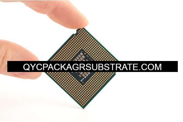
SIP Package Substrate
What are the functions of SIP Package Substrate?
The functions of SIP Package Substrate include:
Providing physical support: Serve as the foundation for electronic components, offering support and protection to assemble them securely together.
Offering electrical connectivity: Enable electrical connections between different components through wires and contact points on the substrate, allowing them to communicate and exchange data.
Heat dissipation management: Absorb, conduct, and dissipate the heat generated by electronic devices through substrate materials and design, ensuring stability and reliability during system operation.
Signal integrity: Minimize signal loss and interference in signal transmission by optimizing wiring and arrangement, ensuring reliable transmission of high-speed electronic signals.
Space-saving: SIP package substrates allow multiple components to be integrated into a compact package, saving space and increasing system integration.
Supporting advanced packaging technologies: Employ advanced packaging techniques such as 3D integration, through-silicon vias (TSVs), etc., to achieve higher performance and smaller package sizes.
In summary, SIP package substrates play a crucial role in integrated circuits and other electronic components, providing various functions to support the performance, reliability, and compact design of the system.
What are the different types of SIP Package Substrate?
There are several different types of SIP (System in Package) package substrates, each tailored to specific applications and requirements. Some common types include:
Organic Substrates: These are made of organic materials such as epoxy resins or fiberglass-reinforced plastics. Organic substrates are cost-effective and widely used in consumer electronics and other applications where cost is a primary consideration.
Ceramic Substrates: Ceramic substrates are made of materials like alumina or aluminum nitride, which offer excellent thermal conductivity and mechanical strength. Ceramic substrates are often used in high-power applications, RF/microwave circuits, and other environments where heat dissipation and reliability are critical.
Silicon Substrates: Silicon substrates are made of silicon wafers and are commonly used in advanced packaging technologies such as system-on-chip (SoC) integration and 3D stacking. Silicon substrates offer high electrical performance and can incorporate features like through-silicon vias (TSVs) for vertical interconnects.
Glass Substrates: Glass substrates are used in applications requiring high precision, such as microelectronics and optoelectronics. Glass substrates offer excellent dimensional stability, low coefficient of thermal expansion, and high transmission of optical signals.
Metal Substrates: Metal substrates are made of materials like aluminum or copper and are used in applications requiring high thermal conductivity and mechanical stability. Metal substrates are commonly used in power electronics, LED lighting, and automotive electronics.
These are just a few examples of the different types of SIP package substrates available. The choice of substrate type depends on factors such as the application requirements, cost considerations, and performance specifications.
What is the relationship between SIP Package Substrate and IC packaging?
The SIP (System in Package) package substrate is a critical component within the broader context of IC (Integrated Circuit) packaging. While IC packaging refers to the overall process of enclosing and protecting integrated circuits within a package, the SIP package substrate specifically refers to the physical foundation or base upon which various components are assembled to create a complete system.
The relationship between SIP package substrates and IC packaging can be understood in several ways:
Integration: SIP package substrates enable the integration of multiple components, including ICs, passive components, and sometimes even MEMS (Micro-Electro-Mechanical Systems), sensors, or antennas, into a single package. This integration enhances system performance, reduces footprint, and simplifies assembly.
Interconnection: The substrate provides a platform for interconnecting the different components within the package. This includes routing electrical signals between ICs, connecting to external pins or balls for input/output (I/O), and providing power and ground distribution.
Thermal Management: Within the context of IC packaging, the substrate plays a crucial role in thermal management by dissipating heat generated by the integrated circuits. This is particularly important for high-performance systems where heat dissipation is a critical factor in ensuring reliability and performance.
Packaging Technology: SIP package substrates often incorporate advanced packaging technologies such as fan-out wafer-level packaging (FOWLP), system-on-chip (SoC) integration, 3D stacking, and through-silicon vias (TSVs). These technologies enable higher levels of integration, improved electrical performance, and enhanced functionality within a compact form factor.
Overall, SIP package substrates are an integral part of IC packaging, enabling the integration, interconnection, and thermal management of components to create highly integrated and efficient systems. They play a crucial role in enabling the development of advanced electronic devices across various applications, from consumer electronics to automotive and aerospace industries.
How does SIP Package Substrate differ from PCB?
SIP (System in Package) package substrate and PCB (Printed Circuit Board) are both essential components in electronic systems, but they serve different purposes and have distinct characteristics. Here are some key differences between SIP package substrates and PCBs:
Function:
SIP package substrate: The primary function of SIP package substrates is to serve as a platform for assembling and interconnecting multiple integrated circuits (ICs), passive components, and other elements to create a complete system in a single package. SIP package substrates focus on providing electrical connectivity, thermal management, and mechanical support for the integrated components.
PCB: PCBs, on the other hand, are standalone boards that provide electrical connectivity between various electronic components, including ICs, resistors, capacitors, and connectors. PCBs serve as the backbone of electronic systems, facilitating the routing of electrical signals between components and providing mechanical support for them.
Integration:
SIP package substrate: SIP package substrates enable high levels of integration by combining multiple components into a single package. This integration helps reduce the overall size of the system, improve performance, and simplify assembly.
PCB: While PCBs also facilitate the integration of electronic components, they typically do not integrate as many components within a single board as SIP package substrates. PCBs are commonly used to connect and mount discrete components and ICs onto a single board.
Complexity:
SIP package substrate: SIP package substrates are often more complex than PCBs, as they incorporate advanced packaging technologies such as 3D integration, through-silicon vias (TSVs), and fan-out wafer-level packaging (FOWLP). These technologies enable higher levels of functionality and performance within a smaller footprint.
PCB: PCBs can vary in complexity depending on the design requirements, but they typically involve simpler fabrication processes compared to SIP package substrates. PCBs are commonly manufactured using processes such as etching, drilling, and soldering.
Application:
SIP package substrate: SIP package substrates are commonly used in applications that require high levels of integration, such as mobile devices, automotive electronics, and networking equipment.
PCB: PCBs are used in a wide range of applications, including consumer electronics, industrial equipment, medical devices, and telecommunications systems.
In summary, while SIP package substrates and PCBs both play essential roles in electronic systems, they differ in terms of function, integration, complexity, and application. SIP package substrates focus on integrating multiple components within a single package, whereas PCBs provide electrical connectivity and mechanical support for individual components mounted on a board.
What are the structure and production technology of SIP Package Substrate?
The structure and production technology of SIP (System in Package) package substrates can vary depending on the specific requirements of the application and the chosen packaging technology. However, here is a general overview of the structure and production technology of SIP package substrates:
Structure:
Substrate Material: SIP package substrates are typically made from various materials, including organic substrates (e.g., epoxy resin or fiberglass-reinforced plastics), ceramic substrates (e.g., alumina or aluminum nitride), silicon substrates, glass substrates, or metal substrates (e.g., aluminum or copper). The choice of substrate material depends on factors such as thermal conductivity, electrical properties, mechanical strength, and cost.
Wiring and Interconnects: The substrate contains a network of wiring traces, vias, and interconnects that facilitate electrical connections between the integrated circuits (ICs), passive components, and other elements mounted on the substrate. Advanced packaging technologies such as through-silicon vias (TSVs) or redistribution layers (RDLs) may be used to enable vertical and horizontal interconnections within the substrate.
Embedded Components: SIP package substrates may incorporate embedded passive components (e.g., resistors, capacitors, inductors) or active components (e.g., transistors, diodes) directly into the substrate material. This integration helps reduce the overall size of the package and improve electrical performance.
Thermal Management Features: To dissipate heat generated by the ICs and other components, SIP package substrates may incorporate thermal vias, heat spreaders, or other thermal management features. These features help improve the reliability and performance of the system by maintaining optimal operating temperatures.
Production Technology:
Substrate Fabrication: The production process begins with the fabrication of the substrate material, which involves processes such as molding, lamination, or deposition, depending on the chosen substrate material. For example, organic substrates may be fabricated using printed circuit board (PCB) manufacturing techniques, while ceramic substrates may be produced using ceramic processing methods.
Wiring and Interconnect Formation: Next, the substrate undergoes processes to create wiring traces, vias, and interconnects. This may involve techniques such as photolithography, etching, or laser drilling to pattern the substrate material and create the desired wiring patterns.
Component Mounting: Once the wiring and interconnects are in place, the ICs, passive components, and other elements are mounted onto the substrate using techniques such as flip-chip bonding, wire bonding, or surface-mount technology (SMT). Advanced packaging technologies such as fan-out wafer-level packaging (FOWLP) or system-on-chip (SoC) integration may be employed to achieve higher levels of integration.
Encapsulation and Testing: Finally, the assembled components are encapsulated within a protective housing or encapsulant material to ensure reliability and protection from environmental factors. The packaged substrate undergoes rigorous testing to verify functionality, electrical performance, and reliability before being deployed in electronic systems.
Overall, the structure and production technology of SIP package substrates are highly versatile, allowing for a wide range of configurations and packaging options to meet the specific requirements of different applications. Advanced packaging technologies continue to evolve, enabling even higher levels of integration, performance, and miniaturization in SIP package substrates.
Frequently Asked Questions (FAQs)
What is a SIP package substrate?
A SIP (System in Package) package substrate is a physical foundation or base upon which integrated circuits (ICs) and other electronic components are assembled to create a complete system within a single package.
What are the functions of SIP package substrates?
SIP package substrates provide electrical connectivity, thermal management, mechanical support, and integration of components within a single package. They also enable high levels of integration, miniaturization, and performance optimization.
How does SIP package substrate differ from PCB?
While both SIP package substrates and PCBs (Printed Circuit Boards) provide electrical connectivity and support for electronic components, SIP package substrates focus on integrating multiple components within a single package, whereas PCBs typically connect discrete components mounted on a board.
What are the different types of SIP package substrates?
Common types of SIP package substrates include organic substrates, ceramic substrates, silicon substrates, glass substrates, and metal substrates. Each type offers different properties and advantages depending on the application requirements.
What are some advanced packaging technologies used in SIP package substrates?
Advanced packaging technologies such as fan-out wafer-level packaging (FOWLP), system-on-chip (SoC) integration, 3D stacking, through-silicon vias (TSVs), and embedded component integration are often employed in SIP package substrates to achieve higher levels of integration, performance, and miniaturization.
What are the applications of SIP package substrates?
SIP package substrates are used in a wide range of applications, including consumer electronics, telecommunications, automotive electronics, medical devices, aerospace, and industrial equipment, where high levels of integration, performance, and miniaturization are required.
Conclusion
In conclusion, SIP (System in Package) package substrates play a crucial role in modern electronics by providing a platform for integrating multiple components into a single package. They enable high levels of integration, miniaturization, and performance optimization, making them essential for a wide range of applications across industries.
SIP package substrates offer various functions, including electrical connectivity, thermal management, mechanical support, and component integration. They come in different types, such as organic, ceramic, silicon, glass, and metal substrates, each with unique properties and advantages depending on the application requirements.
Advanced packaging technologies, such as fan-out wafer-level packaging (FOWLP), system-on-chip (SoC) integration, and through-silicon vias (TSVs), are commonly used in SIP package substrates to achieve higher levels of integration and performance.
Overall, SIP package substrates continue to evolve to meet the demands of emerging technologies and applications, driving innovation and advancement in the field of electronic packaging. Their versatility and functionality make them indispensable components in the development of next-generation electronic systems.