
What is Ultra-small spacing led PCB?
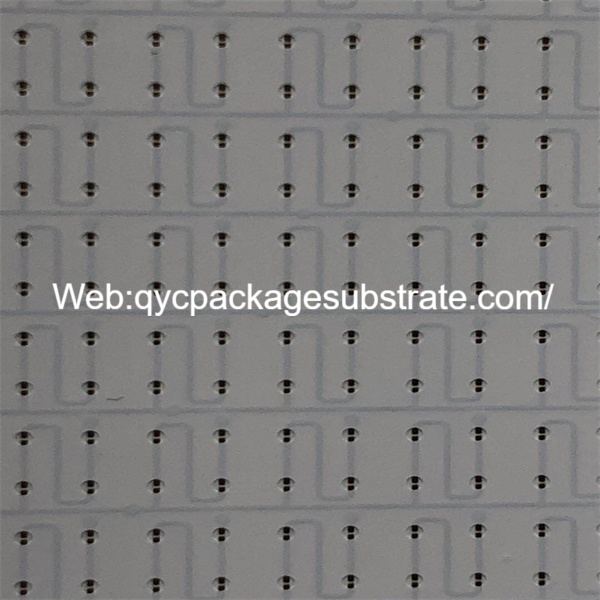
We are a professional Ultra-small spacing led PCB manufacturer, we mainly produce ultra-small bump pitch BGA substrate, ultra-small trace and spacing packaging substrate and LED PCBs from 2 layer to 20 layers.
LED PCB (Printed Circuit Board): LED PCBs are specially designed circuit boards that support and connect LED components. These boards are crucial for providing power and ensuring proper functioning of LEDs in various electronic devices and lighting applications.
Ultra-small spacing: This term likely refers to the distance or spacing between components or features on the PCB. Smaller spacing indicates a more densely populated circuit board, which can be important for miniaturization and compact electronic devices.
Putting it together, an “Ultra-small spacing LED PCB” might suggest a printed circuit board designed for LED applications with a focus on compactness and densely packed components. This could be crucial in applications where space is limited, such as in portable electronics or compact lighting fixtures.
It’s worth noting that technology and terminology can evolve, and new concepts or products may emerge after my last update. If there have been developments in this area since then, I recommend checking the latest sources or industry publications for the most up-to-date information.
What Lies Behind Ultra-Small Spacing LED PCBs?
The technological innovations behind “Ultra-Small Spacing LED PCBs” mainly involve the following aspects:
High-Density Integration: Ultra-small spacing LED PCBs have a higher component density, where LEDs and other electronic components are more tightly integrated. This high integration allows for a more compact circuit board, providing greater design flexibility for applications with limited space.
Miniaturized Design: This type of PCB focuses on minimizing size and weight. By reducing the spacing between components, it enables smaller designs, making products such as LED fixtures or displays more lightweight and portable.
High Performance and Efficiency: Ultra-small spacing LED PCBs are typically designed for high-performance applications, such as high-resolution displays or lighting solutions requiring high brightness. They may employ advanced heat dissipation techniques and efficient power management to ensure the longevity and stability of LED components.
Advanced Materials and Manufacturing Processes: In terms of manufacturing, ultra-small spacing LED PCBs may use advanced materials and manufacturing processes to ensure a highly precise layout and reliability. This may include high-precision printing and assembly technologies.
These technological innovations redefine expectations for compact, high-performance lighting solutions in the following ways:
Space Efficiency: Allows for more LED components in a limited space, providing higher brightness and resolution.
Innovative Design: Designers have greater freedom to implement innovative designs, creating lighting products that are thinner and more sophisticated.
High-Performance Applications: Ideal for applications necessitating high-performance LED solutions, including LED displays, medical imaging equipment, and other products requiring both high integration and a compact design.
It’s important to highlight that the aforementioned description provides a general overview, and specific technical details and innovations can vary depending on the manufacturer and product.
What Critical Functions Do Ultra-Small Spacing LED PCBs Serve?
Ultra-small spacing LED PCBs serve several critical functions in advanced electronic applications beyond LED placement, ensuring optimal electrical connections, thermal management, and structural integrity:
Electrical Connections: Through precision circuit layout design, ultra-small spacing LED PCBs ensure robust electrical connections between LED components. This involves minimizing the distance between conductors and electrical elements to reduce signal transmission resistance and interference, contributing to the stability and reliability of the circuit.
Thermal Management: LEDs generate heat during operation, and effective thermal management is crucial for ensuring the longevity and performance of the LEDs. Ultra-small spacing LED PCBs often incorporate optimized heat dissipation designs, including metal substrates, heat pads, or other thermal materials, to efficiently conduct and disperse heat, preventing LED overheating.
Structural Integrity: The structural integrity of the PCB is essential for the stability and reliability of electronic devices. Ultra-small spacing LED PCBs may utilize high-density interconnect technologies, such as fine traces and microvias, to achieve complex circuit layouts in small form factors. Additionally, structural design considers the impact of mechanical stress, vibration, and temperature fluctuations on the PCB to ensure stable operation in various environmental conditions.
These factors collectively ensure the performance and reliability of ultra-small spacing LED PCBs in advanced electronic applications, making them suitable for scenarios that demand high integration, compact design, and efficient heat dissipation.
How Do Various Package Substrates Contribute to LED Technology?
Various package substrates contribute to LED technology through their unique characteristics. Ceramic, organic, and laminate substrates are common types. Here are their main features and how they enhance the versatility and adaptability of ultra-small spacing LED PCBs:
Ceramic Substrates:
Strong Thermal Conductivity: Ceramic substrates excel in thermal conductivity, efficiently dissipating heat and ensuring the prolonged stability of LEDs.
High Temperature Stability: They excel in maintaining stability in elevated temperatures, rendering them well-suited for applications demanding high brightness and substantial LED power.
High Mechanical Strength: Ceramic substrates typically possess high mechanical strength, reducing the impact of mechanical stress on LEDs.
Organic Substrates:
Lightweight and Flexible: Organic substrates, due to their lightweight and flexibility, are ideal for situations where constraints on weight and size are a primary consideration.
Easy to Process: Easily processed and manufactured, these substrates are ideal for streamlined mass production and quick manufacturing.
Relatively Lower Thermal Conductivity:Unlike ceramics, organic substrates generally have a lower level of thermal conductivity. This implies that for high-power LED applications, there may be a necessity for additional heat dissipation design.
Laminate Substrates:
Cost-Effective: Laminate substrates are usually more cost-effective than ceramic substrates, making them suitable for cost-sensitive applications.
Good Insulation: They have good electrical insulation properties, helping prevent circuit shorts.
Suitable for Medium-Power Applications: Laminate substrates perform well in medium-power LED applications, providing adequate heat dissipation performance.
The suitability of ultra-small spacing LED PCBs depends on specific application requirements. Ceramic substrates are suitable for high-power and high-temperature environments, organic substrates are applicable in scenarios requiring lightweight and flexibility, while laminate substrates are more competitive in cost-sensitive applications. Choosing the right substrate type helps optimize the performance and cost of LED products.
How Does Package Substrate Technology Innovate for LEDs?
Package substrate technology innovations for LEDs are manifested in the following aspects:
Material Selection: New packaging substrate technologies may utilize more advanced materials with improved heat dissipation, conductivity, and mechanical strength. The use of these materials enhances the performance and reliability of LED chips.
Manufacturing Processes: Innovative packaging substrate technologies may employ more sophisticated manufacturing processes to achieve smaller component layouts. This aids in designing ultra-small spacing LED PCBs, making them more suitable for applications with limited space, such as portable electronic devices or compact lighting fixtures.
Heat Dissipation Design: Innovations in packaging substrate technology can improve heat dissipation design, enhancing the heat dissipation efficiency of LED components. This is crucial for the longevity and stability of LED chips.
Connection Technologies: Innovative packaging substrate technologies may introduce new connection technologies, such as High-Density Interconnect (HDI) technology, enabling higher connection density and smaller component spacing.
Thin Film Packaging: Some innovations may include thin film packaging technology, which enables thinner packaging, making LED modules more lightweight.
These innovations contribute to the advancement of LED packaging technology, especially in the context of ultra-small spacing LED PCBs. By adopting more advanced packaging substrate technologies, manufacturers can achieve more efficient, compact, and reliable LED packaging to meet the evolving demands of the market.
How Do Ultra-Small Spacing LED PCBs Differ from Traditional PCBs?
Ultra-small spacing LED PCBs differ from traditional PCBs in several key aspects, mainly due to their specialized design for LED applications:
Size and Density: Ultra-small spacing LED PCBs typically have smaller dimensions and higher component density. LED technology itself is often very compact, so this PCB design allows more LED components to be densely integrated into a smaller space, which is crucial for applications requiring a compact design, such as LED displays.
Heat Dissipation Design: LEDs generate heat when emitting light, so ultra-small spacing LED PCBs may include more sophisticated heat dissipation designs to ensure stable operating temperatures for LED components under high load conditions. This may involve heat sinks, thermal conductive materials, or other heat dissipation solutions.
Power and Current Management: Due to the sensitivity of LEDs to current and voltage, ultra-small spacing LED PCBs may incorporate more advanced power and current management circuits to ensure proper power supply to LED components while maximizing their lifespan.
Signal Integrity: In applications like high-resolution LED displays, ultra-small spacing LED PCBs may require higher signal integrity to ensure reliable data transmission. This may include more complex signal conditioning circuits and shielding designs to reduce signal interference and distortion.
Manufacturing Processes: To meet size and density requirements, the manufacturing processes for ultra-small spacing LED PCBs may differ from traditional PCBs. This could involve higher precision printing and assembly processes.
In summary, ultra-small spacing LED PCBs place more emphasis on aspects such as size, heat dissipation, power management, and signal integrity in their design and manufacturing to meet the demands of high-performance applications like LED displays.
What Defines the Structure of Ultra-Small Spacing LED PCBs?
Factors Defining the Structure of Ultra-Small Spacing LED PCBs:
Component Size and Layout: The key to ultra-small spacing LED PCBs lies in the dimensions and arrangement of components. Small, high-density LED components often require smaller PCB sizes and more compact layouts.
PCB Layer Structure: A multi-layer PCB structure provides more wiring space, aiding in accommodating more components and enhancing circuit integration.
Material Selection: Choices such as the substrate material and copper thickness affect electrical performance and heat dissipation. In ultra-small spacing LED PCBs, high-performance materials may be needed to ensure signal integrity.
Thermal Management: LED components typically generate heat, making effective thermal management a crucial design consideration. This might include the use of heat sinks, thermal pads, and other heat-conductive materials.
Manufacturing Technologies:
High-Density Interconnect (HDI) Manufacturing Technology: HDI technology allows higher component density in smaller spaces. Through the use of fine traces, blind vias, buried vias, and other specialized designs, HDI facilitates reducing the overall size of the PCB.
Semi-Additive Method: This advanced manufacturing technique enables precise addition of thin metal layers on the PCB. This method increases the density of the traces, reducing the spacing between components and achieving a smaller PCB size.
Laser Drilling: Laser drilling is a precision machining technique used to create tiny holes in the PCB, allowing for the placement of more components in smaller areas.
Note: In actual design and manufacturing, designers typically need to carefully optimize and balance aspects such as component layout, PCB layer structure, and heat dissipation design for ultra-small spacing LED PCBs.
What Common Queries Surround Ultra-Small Spacing LED PCBs?
Performance Concerns:
Will ultra-small spacing LED PCBs sacrifice performance? How do they differ from traditional LED PCBs?
The design of ultra-small spacing LED PCBs is typically aimed at achieving higher pixel density and more uniform display. While the compact design may pose challenges for heat dissipation and power distribution, advanced technology and materials help address these issues.
Reliability and Lifespan:
Does the compact arrangement of PCBs affect the lifespan and reliability of LEDs?
Well-designed and manufactured ultra-small spacing LED PCBs should not negatively impact the lifespan of LEDs. In fact, through optimized heat dissipation and power management, these designs may enhance the stability and lifespan of LEDs.
Maintenance and Repair:
Is it more challenging to maintain and repair ultra-small spacing LED PCBs?
Indeed, due to their compact nature, more advanced skills and equipment may be required for repairs. Nevertheless, technological advancements usually lead to manufacturers providing more effective services for maintenance and replacement.
Cost and Availability:
Are ultra-small spacing LED PCBs more expensive? Are they widely available?
While the manufacturing costs for ultra-small spacing LED PCBs may initially be higher, advancements in technology typically lead to cost reductions over time. Although these PCBs are gaining popularity in the market, they might still be pricier compared to conventional LED PCBs.
Technical Standards:
What industry standards exist for ultra-small spacing LED PCBs? How can one ensure that products meet these standards?
Industry standards, including criteria like pixel density and brightness uniformity, are commonly followed by manufacturers. Buyers should select products that align with the specified requirements.
Conclusion: How Do Ultra-Small Spacing LED PCBs Illuminate the Path Forward?
In embracing the future, innovations in ultra-small spacing LED PCBs not only illuminate our surroundings but also light the path forward. The advancements in this technology have positive implications for the development of lighting and electronic devices, and here are some potential impacts:
Space Efficiency: Ultra-small spacing LED PCBs allow for a more compact arrangement of LED components within limited space. This is crucial for lightweight electronic devices and small lighting products, providing designers with greater flexibility.
Energy Efficiency: Small-spacing LED PCBs typically offer higher energy efficiency as they can more effectively manage power and heat dissipation. This helps reduce energy consumption, aligning with sustainability goals.
Innovative Applications: Innovations in ultra-small spacing LED PCBs drive new applications of LED technology in various fields. For instance, they might be used in flexible displays, smart lighting systems, or even embedded medical devices.
Brightness and Color Control: Advances in PCB technology contribute to more precise control of LED brightness and color, offering more personalized and high-quality lighting solutions.
In conclusion, the innovations in ultra-small spacing LED PCBs not only enhance the performance of existing products but also open up new possibilities for the future of lighting and electronic technology. These technological advancements contribute to the creation of smarter, more efficient, and more compact devices, driving the progress of technology while contributing to sustainability goals.