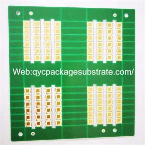
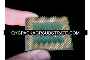
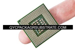
 Fabricante de sustratos Flip-Chip Package
- Teléfono: +086 0755 85241496
- Correo electrónico: service@qycltd.com
Why CHOOSE SHENZHEN QYC CO.,LTD?
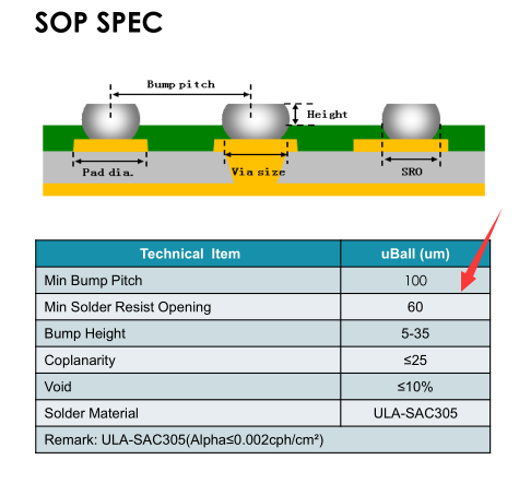
We are a company specializing in the production of small pitch High multilayer(20 layer) semiconductor packaging substrates(The Microtrace/spacing are 9um/9um, and smallest trace/spacing HDI circuit boards( trace/spacing are from 40um/40um). When you see our product column, we were written in the form of an article,Not much production data is written. the main reason is to facilitate the Google network promotion, about the packaging substrate and HDI PCB, if you have any design or production questions, you can contact us at any time, our engineers will reply you Soon. By the way. The types of packaging substrates we mainly produce are: 3D Sustrato del paquete IC, 2.5D Sustrato del paquete IC,2D Sustrato del paquete IC, Sustrato del paquete WLP, FCBGA Package Substrate, Sustrato del paquete POP,Sustrato de paquete CSP, Sustrato de paquete SIP, Sustrato del paquete SOP, Sustrato del paquete PGA,Sustrato del paquete de matriz de rejilla de bolas, Sustrato del paquete LCC, Sustrato del paquete DIP, Sustrato del paquete QFP, Ceramic Package Substrate, High Frequency Package Substrate, Embedded Cavity Package Substrate, and others. Meanwhile. We also have many full set of advanced packaging production lines, we provide advanced packaging services.
In the process of designing Packaging Substrate, if you have doubts about the production process capabilities of the packaging substrate, or are unsure whether the factory can produce the ideal Packaging Substrate according to your design requirements, don't hesitate, you can send us an email at any time . We are always willing to listen to your concerns and needs, and we have a strong team of more than 200 engi
neers dedicated to solving your technical and design problems.
Every month, we welcome nearly 100 to 200 new customers from all over the world. Some of these customers find us through the Internet, and some are recommended by old customers. This extensive international collaboration experience equips us to handle a wide range of different needs and challenges. Our quality is stable and reliable because our equipment has always maintained an advanced level and the materials we use are all high-quality brands specified by our customers.
In our cooperation, our goal is to ensure that each customer receives the highest level of service and products. We firmly believe that through active collaboration, we can jointly drive project success and achieve excellence in Packaging Substrate design and manufacturing.
No matter how complex your challenges are, we are willing to work with you to create outstanding solutions that bring your projects to life. We look forward to establishing a close working relationship with you and providing you with professional support and advice.
Global Flip Chip Package Substrate
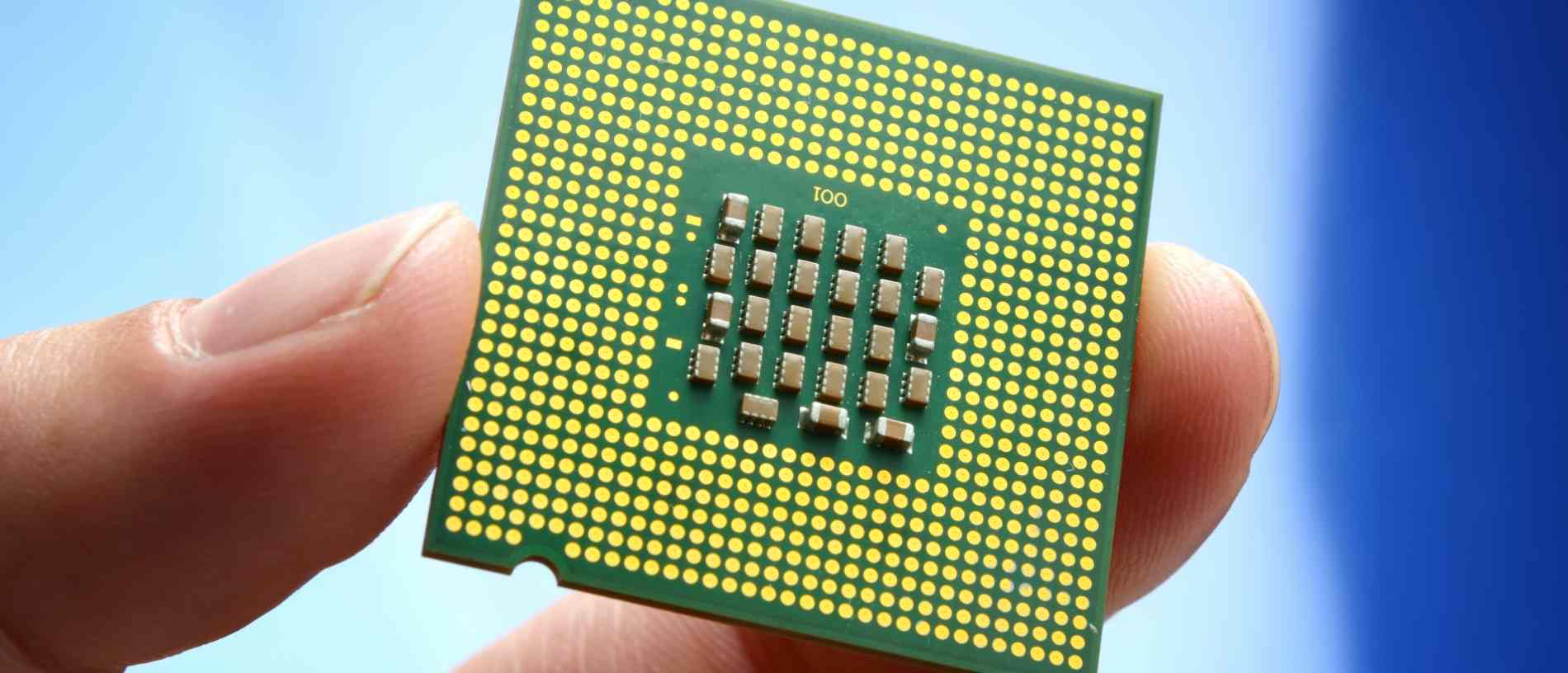
In the ever-evolving world of electronics manufacturing, precision and reliability cannot be compromised. SHENZHEN QYC CO., LTD are a professional Flip Chip Package Substrate production company
With over 10,000 dedicated employees and cutting-edge equipment sourced exclusively from Japan, we pride ourselves on consistently delivering high-quality FC BGA substrates. Quality assurance is the cornerstone of our operations. Our high-precision equipment carefully sourced from Japan is the backbone of our commitment to providing best-in-class FC BGA substrate. The result is a level of quality and stability that our customers can fully trust.
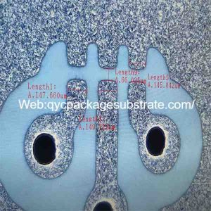
Our production capabilities cover a wide range of designs, ranging from 4- to 20 layer Flip Chip Package Substrate. Whether your project requires a compact design or a multi-layer solution, our expertise and infrastructure are tailored to your needs. What sets us apart is our ability to work with exceptional precision, with a minimum line width of 9 um and a minimum pitch of 9 um.
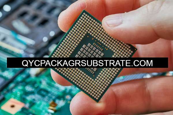
Flip Chip Packaging Substrate
Our production turnaround time is excellent, typically 1 to 2 months. Despite the speed at which we produce, quality is always our primary focus. We firmly believe that quality cannot be compromised, even under tight schedules. Each project undergoes strict quality control and testing procedures to ensure that every Package Substrate produced has exceptional performance and reliability. This rapid delivery is harmoniously combined with an unwavering commitment to adhering to the highest quality standards, ensuring your project runs smoothly and seamlessly.
In the process of manufacturing Sustrato del paquete, material selection is crucial. We offer a wide variety of packaging substrate materials, most of which come from Asia, including Japan, South Korea, Taiwan and China. We deeply understand that every project is unique, so we will be flexible in selecting and using the most suitable materials based on the needs of our customers to ensure that the Package Substrate produced perfectly meets the specific requirements of the project.
Our goal is to provide excellent solutions, promote the continuous development of the electronics industry, and create greater value for customers. We look forward to working with you to achieve project success.
FC-BGA substrates
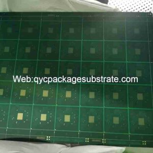
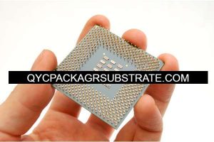
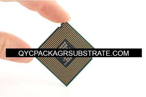
FC-BGA (Flip Chip Ball Grid Array) is a semiconductor packaging technology that plays an important role in high-density semiconductor packaging, allowing high-speed chips to have more functions. This technology is critical to many industries such as servers, artificial intelligence, networking, communications, military and aviation. Product types:IC Substrates. FC-BGA substrates. SHDBU substrates. FC-CSP Substrates. CPCORE Substrates. Module Substates. MSD substrates, FR substrates, SEN substrates , MIC substrates and others.By using FC-BGA, we are able to achieve higher integration and performance.
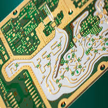
In high-density packaging, multi-layer substrates are essential, such as the high multi-layer substrates we manufacture with 10 to 20 layers. These substrates are suitable for small pitch and small line width requirements, and we adopt Msap or Sap technology to meet the current requirements of semiconductor micro-manufacturing. These high multilayer substrates provide a solid foundation for high-performance chips, ensuring their reliability and stability in a variety of applications.
In addition to high-density substrate manufacturing, we provide comprehensive support from substrate design to production and packaging. This means we can provide our customers with a one-stop solution to meet their specific needs. Not only that, we are also able to use high-frequency materials to adapt to areas requiring high-frequency performance such as communication products, ensuring the stability and reliability of products in high-frequency environments.
Our technologies and products cover multiple key areas and support various industries to meet the high density, high performance and high reliability requirements of modern electronic equipment.
-
Flip Chip Chip Scale Package Substrates Manufacturer
Flip Chip Chip Scale Package Substrates Manufacturer Flip Chip Chip Scale Package Substrates Manufacturer,Flip Chip Chip Scale Package (FCCSP) substrates are advanced interconnection platforms used in semiconductor packaging. They facilitate the direct ... -
Ajinomoto(ABF) Filp Chip Substrate Manufacturer
Ajinomoto(ABF) Filp Chip Substrate Manufacturer Ajinomoto(ABF) Filp Chip Substrate Manufacturer,Ajinomoto (ABF) Flip Chip Substrates are high-performance circuit boards designed for advanced flip chip packaging. ABF, or Ajinomoto Build-up Film, is ... -
SiP(System in Package) Substrate Manufacturer
SiP(System in Package) Substrate Manufacturer SiP(System in Package) Substrate Manufacturer,SiP (System in Package) Substrates are advanced circuit boards designed to integrate multiple semiconductor components into a single package, providing a ... -
Ultrathin High Speed Substrates Manufacturer
Ultrathin High Speed Substrates Manufacturer Ultrathin High Speed Substrates Manufacturer,Ultrathin High-Speed Substrates are advanced circuit board materials engineered for high-frequency applications requiring minimal thickness without compromising performance. These substrates are ...
