
Ultra-small Size BGA Substrates Manufacturer
Ultra-small Size BGA Substrates Manufacturer,Ultra-small size BGA (Ball Grid Array) Substrates are advanced components designed for compact electronic devices requiring high-density integration. These substrates feature a minimized footprint and fine pitch interconnects, allowing for efficient use of board space while maintaining structural integrity. Engineered with advanced materials like thin-film polymers or specialized ceramics, they offer superior thermal management and electrical insulation properties crucial for small form factor designs. Ultra-small size BGA Substrates support the miniaturization trend in modern electronics, including smartphones, tablets, and wearable technology, where space optimization is essential. Their precise manufacturing ensures reliable performance and durability in demanding applications.
What is Ultra-small Size BGA Substrates?
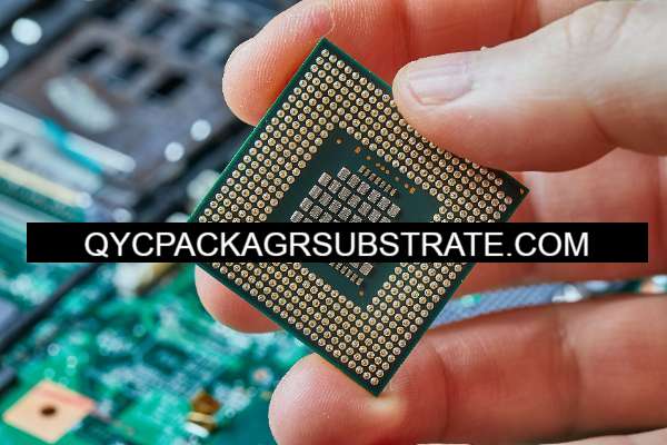
Ultra-small Size BGA (Ball Grid Array) substrates are specialized circuit board designs used in advanced packaging solutions for integrated circuits (ICs). These substrates are characterized by their compact size and high-density interconnections, allowing for efficient electrical performance and thermal management. They are typically employed in applications where space is at a premium, such as mobile devices, wearables, and compact consumer electronics.
The design of Ultra-small Size BGA substrates includes a grid of solder balls on the bottom side, which serve as connection points to the PCB. This arrangement facilitates a more uniform distribution of thermal and electrical properties, enhancing the overall reliability of the component. The substrates are manufactured using advanced materials and processes, often involving techniques like microvias and high-density interconnects (HDI) to achieve the necessary precision and density.
One of the significant advantages of Ultra-small Size BGA substrates is their ability to support higher pin counts in a smaller footprint, which is critical for modern electronic devices that require robust performance in limited space. Additionally, these substrates offer improved electrical performance due to shorter signal paths and reduced inductance.
As the demand for miniaturization in electronics continues to grow, Ultra-small Size BGA substrates play a crucial role in enabling innovative designs and enhancing the functionality of next-generation devices. Their ability to combine size efficiency with high performance makes them a preferred choice for manufacturers in the semiconductor and electronics industries.
Ultra-small Size BGA Substrates Manufacturer
What are the Ultra-small Size BGA Substrates Design Guidelines?
Designing Ultra-small Size BGA substrates involves several key guidelines to ensure optimal performance, reliability, and manufacturability. Here are the essential design considerations:
- Layer Stack-Up:Optimize the layer stack-up to balance electrical performance and mechanical stability. Use fewer layers if possible, but ensure adequate routing for power and ground planes.
- Pad Size and Layout: Maintain appropriate pad sizes for solder balls to ensure reliable connections. The pad design should accommodate the specific solder ball size, typically ranging from 0.3 mm to 0.6 mm in diameter.
- Microvias and HDI: Utilize microvias and high-density interconnect (HDI) techniques to maximize routing density. These features help achieve compact designs while maintaining signal integrity.
- Signal Integrity: Pay attention to trace widths and spacing to minimize crosstalk and maintain signal integrity. Employ controlled impedance routing for high-speed signals, and consider differential pairs where applicable.
- Thermal Management:Incorporate thermal vias and heat sinks to manage heat dissipation effectively, especially for power-hungry components. Consider using thermal relief pads for better heat distribution.
- Assembly Considerations: Design for manufacturability by ensuring proper spacing for solder paste application and adequate clearance for component placement. Consider the reflow profile and assembly process during design.
- Testing Access: Include test pads or access points for in-circuit testing (ICT) or functional testing to facilitate quality assurance and troubleshooting.
- Design Rule Check (DRC): Rigorously perform DRC to ensure that all design rules regarding trace widths, spacing, and pad sizes are adhered to, minimizing the risk of defects during fabrication.
- Material Selection: Choose suitable substrate materials that offer the required electrical properties and thermal conductivity, such as FR-4 or high-frequency laminates, depending on the application.
By following these design guidelines, engineers can create effective Ultra-small Size BGA substrates that meet the demands of modern electronics, ensuring high performance and reliability in compact spaces.
What is the Ultra-small Size BGA Substrates Fabrication Process?
The fabrication process for Ultra-small Size BGA (Ball Grid Array) substrates involves several critical steps to ensure high precision and reliability. Here’s an overview of the typical fabrication process:
- Material Selection: Start with selecting appropriate substrate materials, such as FR-4 or high-frequency laminates, based on electrical performance and thermal management requirements.
- Layer Preparation: The process begins with layering the substrate materials. Layers are stacked according to the designed layer stack-up, including dielectric layers and conductive planes.
- Imaging and Etching: Photolithography is used to transfer the circuit design onto the substrate. A photosensitive film is applied, exposed to UV light through a mask, and then developed. This creates a pattern that is etched away to form the copper traces and pads.
- Drilling and Via Formation: Microvias and traditional vias are drilled into the substrate using laser or mechanical drilling techniques. These vias allow for inter-layer connections and high-density routing.
- Plating: After drilling, the vias are plated with copper to create conductive paths. This process typically involves electroless copper deposition followed by electrolytic plating to achieve the desired thickness.
- Solder Mask Application: A solder mask layer is applied to protect the circuitry and define areas for soldering. This helps prevent solder bridging during assembly.
- Surface Finish: A surface finish, such as immersion gold or OSP (Organic Solderability Preservative), is applied to the pads to enhance solderability and protect against oxidation.
- Ball Placement: Solder balls are attached to the pads using techniques like stencil printing or placement. The balls are typically solder spheres made from alloys like SAC (Tin-Silver-Copper).
- Reflow Process: The substrate undergoes a reflow process where the solder balls are melted and bonded to the pads. This is done in a controlled environment to ensure proper solder joint formation.
- Testing and Inspection: Finally, the substrates are tested for electrical integrity, solder joint quality, and overall functionality. Inspection methods may include X-ray imaging and Automated Optical Inspection (AOI).
By following these steps, manufacturers can produce Ultra-small Size BGA substrates that meet stringent performance and reliability standards, suitable for high-density electronic applications.
How do you manufacture Ultra-small Size BGA Substrates?
Manufacturing Ultra-small Size BGA (Ball Grid Array) substrates involves a series of precise steps to ensure high quality and performance. Here’s a detailed overview of the manufacturing process:
- Material Selection: Choose suitable substrate materials, such as FR-4 or high-frequency laminates, based on electrical and thermal requirements.
- Layer Preparation: Stack the layers according to the designed layer stack-up, including dielectric materials and copper planes.
- Photolithography: Apply a photosensitive resist on the substrate. Use photomasks to expose the resist to UV light, defining the circuit pattern. Develop the resist to reveal the desired circuit layout.
- Etching: Remove unwanted copper using chemical etching. This process creates the necessary traces and pads on the substrate.
- Drilling: Drill holes for vias using laser or mechanical drilling methods. These vias are essential for interconnecting layers.
- Plating: Plate the drilled vias with copper through electroless and electrolytic plating processes, ensuring sufficient thickness for conductivity.
- Solder Mask Application: Apply a solder mask layer to protect the circuitry and define soldering areas. This helps prevent solder bridging during assembly.
- Surface Finish: Apply a surface finish such as immersion gold or OSP to enhance solderability and protect pads from oxidation.
- Solder Ball Placement: Use stencil printing or placement techniques to attach solder balls to the pads. Ensure accurate alignment for reliable connections.
- Reflow Process: Heat the substrate in a reflow oven to melt the solder balls, forming strong bonds with the pads. This step is critical for achieving reliable solder joints.
- Testing and Inspection: Conduct electrical testing, X-ray inspection, and Automated Optical Inspection (AOI) to verify solder joint integrity and overall functionality.
- Final Assembly: The manufactured substrates can then be integrated into electronic devices, ensuring compatibility with assembly processes.
By following these steps, manufacturers can produce Ultra-small Size BGA substrates that meet the demands of compact, high-performance electronics.
How much should Ultra-small Size BGA Substrates cost?
The cost of Ultra-small Size BGA (Ball Grid Array) substrates can vary significantly based on several factors, including:
- Material Type: High-performance materials may cost more than standard options.
- Layer Count: More complex designs with multiple layers typically increase manufacturing costs.
- Quantity: Larger production runs usually result in lower per-unit costs due to economies of scale.
- Design Complexity: More intricate designs with microvias and HDI features can lead to higher prices.
- Assembly Services: If additional assembly services are included, this can impact overall costs.
Generally, the price range for Ultra-small Size BGA substrates can be anywhere from a few dollars per unit to over $20 or more for highly specialized or low-volume orders. For precise pricing, it’s best to consult with manufacturers or suppliers, as they can provide quotes based on specific design requirements and quantities.
What is Ultra-small Size BGA Substrates base material?
The base material for Ultra-small Size BGA (Ball Grid Array) substrates is typically chosen based on the specific electrical, thermal, and mechanical requirements of the application. Commonly used base materials include:
- FR-4: A widely used epoxy-based laminate that offers a good balance of cost, performance, and thermal stability. Suitable for many general-purpose applications.
- High-Frequency Laminates: Materials like Rogers or Taconic are used for applications requiring excellent signal integrity, low loss, and high thermal stability, often in RF and microwave applications.
- Polyimide:This material offers high thermal resistance and flexibility, making it suitable for applications with demanding thermal conditions or where conformability is important.
- Ceramic Materials: In high-performance applications, ceramics can be used for their superior thermal and electrical properties, though they are typically more expensive.
- High-Density Interconnect (HDI) Materials: These are specifically designed for high-density applications and may include various combinations of dielectric materials and reinforced structures.
The choice of base material is crucial as it impacts the substrate’s performance characteristics, including thermal conductivity, dielectric constant, and mechanical strength.
Which company makes Ultra-small Size BGA Substrates?
In the electronics industry, several companies specialize in manufacturing Ultra-small Size BGA (Ball Grid Array) substrates. These companies typically possess advanced manufacturing technologies and extensive industry experience to meet the market’s demand for high-performance, high-density electronic products. Here are some well-known manufacturers:
- TSMC (Taiwan Semiconductor Manufacturing Company): As the world’s largest semiconductor foundry, TSMC not only produces chips but also offers related packaging and substrate solutions, including Ultra-small Size BGA substrates.
- Intel: Intel manufactures not only processors but also develops and produces various high-performance substrates for its advanced processor series.
- ASE Group: As a leading semiconductor packaging and testing services company, ASE Group provides a variety of packaging solutions, including BGA substrates.
- Foxconn: Foxconn is renowned in the electronic manufacturing sector, offering various electronic components and substrate manufacturing services, including Ultra-small Size BGA substrates.
- Unimicron: Unimicron focuses on high-tech PCBs and packaging substrates, providing a range of high-density substrates, including Ultra-small Size BGA.
These companies utilize advanced manufacturing techniques and materials to produce high-quality Ultra-small Size BGA substrates, meeting the needs of various industries.
At the same time, our company also has the capability to produce Ultra-small Size BGA substrates. We have modern manufacturing facilities and a top-notch technical team that can provide customized solutions based on the specific needs of our customers. Our Ultra-small Size BGA substrates use high-performance materials, such as FR-4 and high-frequency laminates, ensuring reliability and stability in high-density applications.
We emphasize quality control at every stage of the manufacturing process, from material selection and pattern transfer to final solder ball installation. We also offer electrical performance testing and visual inspection to ensure that every substrate meets industry standards.
Additionally, we are committed to closely collaborating with our customers to understand their needs and application scenarios, providing the most suitable product solutions. Whether for mass production or small batch customization, we can respond flexibly to meet our customers’ requirements for high quality and rapid delivery.
Through our professional technology and rich experience, our company has achieved significant success in the manufacturing of Ultra-small Size BGA substrates, providing reliable products and high-quality services that help our customers stand out in a competitive market.
What are the 7 qualities of good customer service?
Good customer service is essential for maintaining customer satisfaction and loyalty. Here are seven key qualities that characterize effective customer service:
- Responsiveness: Quickly addressing customer inquiries and concerns demonstrates respect for their time and needs. Timely responses help build trust and satisfaction.
- Empathy: Understanding and acknowledging customers’ feelings and perspectives can enhance the service experience. Empathy shows that the service representative cares about the customer’s situation.
- Knowledgeability:Customer service representatives should have a deep understanding of the products or services offered. This knowledge allows them to provide accurate information and effective solutions.
- Patience:Dealing with frustrated or confused customers requires patience. Taking the time to listen and explain solutions thoroughly can lead to a more positive experience.
- Clear Communication: Using simple, clear language and avoiding jargon ensures customers understand the information provided. Good communication fosters a better customer experience.
- Positive Attitude: A friendly and positive demeanor can significantly impact the customer’s experience. Enthusiasm and a willingness to help can create a welcoming atmosphere.
- Follow-Up: After resolving an issue or inquiry, following up with the customer shows that the company values their feedback and wants to ensure their satisfaction. This can help build long-term relationships.
These qualities work together to create a supportive and effective customer service experience, enhancing customer loyalty and satisfaction.
FAQs
What is an Ultra-small Size BGA substrate?
Ultra-small Size BGA substrates are compact circuit board designs used for high-density electronic applications. They feature a grid of solder balls on the underside, allowing for efficient electrical connections in a small footprint.
What materials are used for Ultra-small Size BGA substrates?
Common materials include FR-4, high-frequency laminates, polyimide, and ceramic materials, chosen based on the specific electrical and thermal requirements of the application.
What are the advantages of using Ultra-small Size BGA substrates?
They offer high pin counts in a smaller space, improved electrical performance due to shorter signal paths, and enhanced thermal management capabilities.
In which applications are Ultra-small Size BGA substrates commonly used?
These substrates are commonly used in mobile devices, wearables, compact consumer electronics, and high-performance computing applications.
How are Ultra-small Size BGA substrates manufactured?
The manufacturing process includes material selection, layer preparation, photolithography, etching, drilling, plating, solder mask application, solder ball placement, and reflow.
What is the typical cost range for Ultra-small Size BGA substrates?
Prices can vary widely based on factors such as material, layer count, design complexity, and quantity ordered, typically ranging from a few dollars to over $20 per unit.
What design guidelines should be followed for Ultra-small Size BGA substrates?
Key guidelines include optimizing layer stack-up, maintaining appropriate pad sizes, using microvias, ensuring signal integrity, and considering thermal management needs.