
ABF Package Substrate Manufacturer
ABF Package Substrate Manufacturer,ABF Package Substrate is an advanced organic packaging substrate manufactured using Advanced Colloidal Copper (ACF) technology. It is lightweight and offers excellent electrical properties and thermal stability, catering to the packaging needs of high-density and high-speed electronic devices. ABF Package Substrate is extensively used in semiconductor packaging and system integration, supporting advanced chip connection technologies such as FCBGA and LGA, to provide outstanding signal transmission and thermal management capabilities for modern electronic products. This substrate plays a crucial role in telecommunications, computing, consumer electronics, and automotive electronics, driving advancements in device miniaturization, performance, and reliability.
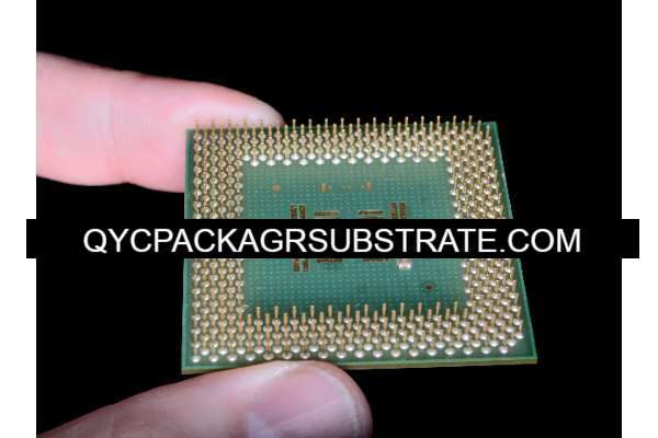
What is ABF Package Substrate?
ABF (Ajinomoto Build-up Film) Package Substrate is a type of advanced packaging substrate used in semiconductor devices and integrated circuits (ICs). It is known for its high performance in terms of electrical and thermal properties, making it suitable for demanding applications in modern electronics.
ABF substrates are typically composed of multiple layers of insulating material (polyimide or similar films) with fine copper circuit patterns. These substrates provide excellent reliability, high-density interconnections, and good signal integrity, crucial for high-speed and high-frequency applications. They are often used in flip-chip packages, ball grid arrays (BGAs), and other advanced packaging technologies.
Key features of ABF package substrates include low dielectric constant (permitting high-speed signal transmission), low moisture absorption (ensuring long-term reliability), and compatibility with fine pitch and high-density interconnects. The manufacturing process involves building up layers of insulating films and conductive traces through processes like lamination, laser drilling, and plating.
Overall, ABF package substrates play a critical role in enabling the miniaturization, performance, and reliability of modern semiconductor devices, making them indispensable in the electronics industry’s quest for smaller, faster, and more efficient products.
ABF Package Substrate Manufacturer
What are the ABF Package Substrate Design Guidelines?
Design guidelines for ABF (Ajinomoto Build-up Film) Package Substrates focus on ensuring optimal performance, reliability, and manufacturability. Here are some key guidelines typically considered:
- Layer Stackup Design: Define the number of layers and their sequence based on the electrical and thermal requirements of the package. Consider the placement of power and ground planes for signal integrity and noise reduction.
- Material Selection:Choose appropriate materials for the substrate layers and bonding films to meet thermal management needs, mechanical strength, and compatibility with assembly processes.
- Routing and Trace Design:Use controlled impedance design techniques to ensure signal integrity. Minimize signal skew and crosstalk by carefully routing high-speed signal traces. Maintain adequate spacing and clearance between traces to prevent electrical interference.
- Via Design:Optimize via placement and design to minimize signal loss, impedance mismatch, and thermal stress. Use microvias or through vias based on density and pitch requirements.
- Thermal Management: Incorporate thermal vias and conductive pads to enhance heat dissipation from heat-generating components. Ensure the substrate material has sufficient thermal conductivity for efficient heat transfer.
- Mechanical Considerations: Design the substrate to withstand mechanical stresses during assembly, thermal cycling, and operation. Ensure adequate stiffness and dimensional stability to prevent warpage or mechanical failures.
- Manufacturability: Design for manufacturability by considering the capabilities and limitations of the fabrication processes (e.g., lamination, laser drilling, plating). Specify clear design rules for tolerances, feature sizes, and registration alignment.
- Reliability and Testing: Include provisions for reliability testing and qualification according to industry standards (e.g., IPC standards). Test for electrical continuity, insulation resistance, thermal cycling, and mechanical durability.
By adhering to these design guidelines, engineers can optimize the performance, reliability, and manufacturability of ABF package substrates, ensuring they meet the stringent requirements of modern electronic devices and applications.
What is the ABF Package Substrate Fabrication Process?
The fabrication process of ABF (Ajinomoto Build-up Film) Package Substrates involves several key steps to achieve the desired electrical, thermal, and mechanical properties:
- Material Preparation:Select and prepare the substrate materials, typically polyimide films and copper foils. These materials should meet the specified electrical and mechanical requirements.
- Layer Lamination:Start by laminating multiple layers of polyimide films together with adhesive bonding films (typically thermosetting resins). This forms the basic substrate structure with alternating insulating and conductive layers.
- Laser Drilling: Use laser drilling techniques to create vias (holes) through the substrate layers where electrical connections are needed. This process ensures precise placement and minimal damage to surrounding materials.
- Via Formation: Plate the vias with conductive material (usually copper) to establish electrical connections between different layers. The plating process can involve several steps, including surface activation, electroless plating, and electrolytic plating.
- Circuit Patterning: Apply photoresist and use photolithography techniques to define circuit patterns on the substrate’s surface. Etch away excess copper to form the desired conductive traces and pads.
- Surface Finish: Apply a surface finish to protect the copper traces from oxidation and to facilitate soldering during assembly. Common surface finishes include ENIG (Electroless Nickel Immersion Gold), OSP (Organic Solderability Preservatives), and HASL (Hot Air Solder Leveling).
- Quality Control and Testing: Conduct rigorous quality checks throughout the fabrication process. Inspect for defects such as shorts, opens, and dimensional inaccuracies. Test the substrate for electrical continuity, insulation resistance, and thermal performance.
- Final Inspection and Packaging: Once fabrication is complete and the substrates pass quality control tests, package them appropriately to protect against contamination and damage during storage and transportation.
By following these steps, manufacturers can produce ABF package substrates that meet the stringent requirements of high-performance electronic applications, ensuring reliability and consistency in electrical connectivity and thermal management.
How do you manufacture ABF Package Substrate?
Manufacturing ABF (Ajinomoto Build-up Film) Package Substrates involves a series of intricate processes designed to create high-performance, reliable substrates for advanced semiconductor packaging. Here’s a detailed overview of the manufacturing process:
- Material Selection and PreparationBegin by selecting high-quality polyimide films and copper foils. The polyimide films serve as the insulating layers, while copper foils provide the conductive paths. These materials are chosen based on their electrical properties, thermal stability, and mechanical strength.
- Layer Lamination:The manufacturing process starts with layer lamination. Polyimide films are stacked together with bonding films (adhesive layers) between them. These bonding films, often thermosetting resins, are essential for creating strong, durable bonds between the polyimide layers. The stackup configuration is determined based on the substrate’s required number of signal and plane layers.
- Laser Drilling:After lamination, the next step is laser drilling. High-precision lasers are used to drill microvias or through-holes (vias) through the layered substrate. These vias will later be filled with conductive material to establish electrical connections between different layers. Laser drilling ensures precise placement and minimal thermal damage to the substrate materials.
- Via Formation:Following laser drilling, the vias are processed to make them conductive. The vias are typically electroplated with copper to form a conductive pathway from one layer to another. This involves several steps:
– Surface Activation: The inner walls of the vias are activated to promote adhesion of the subsequent copper layers.
– Electroless Copper Deposition: A thin layer of copper is deposited over the activated surface to initiate the plating process.
– Electrolytic Copper Plating: Copper is electrodeposited into the vias to build up sufficient thickness for electrical conductivity.
- Circuit Patterning:Once vias are formed and plated, the substrate undergoes circuit patterning. A photoresist layer is applied and exposed to UV light through a photomask, defining the circuit patterns. The exposed areas are then etched away to reveal the copper traces and pads that will carry electrical signals and connections.
- Surface Finish Application:After circuit patterning, a surface finish is applied to protect the exposed copper traces and pads. Common surface finishes include:
– ENIG (Electroless Nickel Immersion Gold): Provides excellent oxidation resistance and solderability.
– OSP (Organic Solderability Preservatives): Protects copper surfaces from oxidation prior to assembly.
– HASL (Hot Air Solder Leveling): Applies a layer of solder to facilitate soldering during assembly.
- Quality Control and Testing:Throughout the manufacturing process, rigorous quality control measures are implemented. Inspections are conducted to detect defects such as shorts, opens, and dimensional inaccuracies. Electrical testing verifies the substrate’s functionality, ensuring proper connectivity and insulation resistance.
- Final Inspection and Packaging:Once fabrication is complete and quality tests are passed, the ABF package substrates undergo final inspection. They are carefully packaged to protect against contamination and physical damage during storage and transportation to assembly facilities.
- Assembly and Integration:ABF package substrates are then assembled with semiconductor devices using advanced packaging techniques such as flip-chip bonding or wire bonding. They provide essential electrical interconnections and thermal management for integrated circuits, ensuring reliable performance in demanding applications.
By following these detailed manufacturing processes, manufacturers produce ABF package substrates that meet the stringent requirements of high-performance electronic devices, contributing to advancements in semiconductor technology and electronic product miniaturization.
How much should ABF Package Substrate cost?
The cost of ABF (Ajinomoto Build-up Film) Package Substrates can vary significantly depending on several factors:
- Size and Complexity: Larger substrates with more layers and complex designs require more materials and processing steps, increasing their cost.
- Materials Used: The choice of polyimide films, copper foils, bonding films, and surface finishes affects the substrate’s cost. High-quality materials with superior electrical and thermal properties typically command higher prices.
- Manufacturing Process: The complexity of the manufacturing process, including lamination, laser drilling, via filling, circuit patterning, and surface finishing, influences costs. Processes requiring high precision and advanced equipment may increase production expenses.
- Volume and Scale: Economies of scale play a significant role in pricing. Larger production volumes often lead to lower per-unit costs due to efficiencies in material usage and manufacturing.
- Customization and Specifications: Customized designs or special requirements such as specific impedance control, thermal management features, or reliability testing standards can affect costs.
- Supplier and Market Conditions: Pricing can vary among different suppliers and regions based on competition, technological capabilities, and market demand.
As of the current market conditions, ABF package substrates are typically priced in a range that reflects their advanced features and performance benefits compared to conventional substrates like FR-4 or ceramic. For precise pricing, contacting suppliers or manufacturers directly with detailed specifications and volume requirements would provide the most accurate estimate.
What is ABF Package Substrate base material?
ABF (Ajinomoto Build-up Film) Package Substrates primarily use polyimide as the base material for their construction. Polyimide is a versatile polymer known for its excellent thermal stability, mechanical strength, and electrical insulation properties, making it ideal for high-performance semiconductor packaging.
Polyimide films used in ABF substrates are engineered to withstand the rigorous demands of modern electronics, including high operating temperatures, mechanical stress during assembly, and reliability over the product’s lifecycle. These films are typically laminated together with adhesive bonding films (such as thermosetting resins) to form multiple layers in the substrate structure.
The choice of polyimide as the base material in ABF substrates allows for:
– High Temperature Resistance: Polyimide films can withstand temperatures ranging from -200°C to +300°C, making them suitable for applications where thermal management is critical.
– Mechanical Stability: They offer good dimensional stability and resistance to mechanical stress, ensuring reliable performance under various operating conditions.
– Electrical Insulation: Polyimide provides excellent electrical insulation properties, essential for maintaining signal integrity and preventing electrical interference in high-speed circuits.
In addition to polyimide, ABF substrates also incorporate copper foils for conducting paths and via connections. These materials together form a robust foundation that supports the intricate circuit patterns and interconnections required in advanced semiconductor packaging technologies.
Which companies make ABF Package Substrate?
ABF (Ajinomoto Build-up Film) package substrates are a key technology in advanced semiconductor packaging, and several renowned companies specialize in manufacturing these substrates, including:
- Nitto Denko Corporation: This company is one of the main producers of ABF substrate materials, providing high-performance polyimide films and related materials.
- Sumitomo Electric Industries, Ltd.: Known for its leadership in high-performance electronic materials, Sumitomo Electric’s products are widely used in ABF package substrates.
- Shinko Electric Industries Co., Ltd.: Specializing in semiconductor packaging substrates, Shinko Electric offers high-quality ABF substrates that meet the demands of high-density interconnects and high-speed signal transmission.
- Nan Ya Plastics Corporation: As a major supplier of plastics and electronic materials, Nan Ya Plastics provides multilayer materials used in ABF substrates.
- TSMC (Taiwan Semiconductor Manufacturing Company): As a global leader in semiconductor manufacturing, TSMC is also involved in producing ABF package substrates to support its chip packaging needs.
Our company has extensive experience in the manufacturing of ABF package substrates, providing high-quality products and custom services. Our production processes strictly adhere to industry standards, ensuring that each substrate meets the technical specifications and performance requirements of our clients. We use the most advanced materials and processes to ensure that the substrates exhibit excellent signal integrity and thermal management performance in high-speed, high-frequency applications.
Additionally, our R&D team continuously invests in innovation to enhance the performance and reliability of our substrates, offering superior solutions to our customers. Whether it’s high-density interconnects or complex circuit designs, we can provide flexible design and manufacturing services tailored to our clients’ specific needs.
By collaborating with us, customers can gain a competitive advantage in the market. We are committed to being a trusted partner, offering comprehensive support and services.
What are the qualities of good customer service?
Good customer service is characterized by several key qualities that contribute to a positive and satisfying experience for customers. These qualities include:
- Responsiveness: Addressing customer inquiries, concerns, and requests promptly and effectively. This includes timely responses to emails, phone calls, and messages.
- Empathy: Understanding and showing empathy towards customers’ needs and emotions. Empathetic customer service representatives can build rapport and trust with customers.
- Clarity: Providing clear and concise information to customers, avoiding jargon or technical language that may confuse them. Clear communication helps customers understand solutions or next steps.
- Problem-solving Skills:Having the ability to identify issues and find solutions efficiently. This may involve troubleshooting technical problems, resolving complaints, or addressing customer dissatisfaction.
- Professionalism: Maintaining a professional demeanor in all interactions with customers. This includes being courteous, respectful, and maintaining composure, even in challenging situations.
- Knowledgeability: Having a good understanding of products or services offered, as well as company policies and procedures. Knowledgeable customer service representatives can provide accurate information and guidance.
- Adaptability: Being flexible and adaptable to different customer preferences and needs. This may involve adjusting communication styles, offering alternative solutions, or accommodating special requests.
- Follow-up: Following up with customers to ensure their issues have been resolved satisfactorily. This demonstrates proactive customer care and reinforces a commitment to customer satisfaction.
- Personalization: Tailoring interactions to the individual customer’s situation or history with the company. Personalized service can make customers feel valued and appreciated.
- Consistency: Providing consistent service experiences across all channels and interactions. Consistency helps build trust and reliability with customers.
Overall, good customer service is about creating a positive customer experience by being responsive, empathetic, knowledgeable, and professional. It involves not only resolving issues but also building relationships and fostering customer loyalty.
FAQs
What is ABF Package Substrate?
ABF Package Substrate is a type of advanced packaging substrate used in semiconductor devices. It consists of multiple layers of polyimide films and copper traces that provide electrical connections and thermal management for integrated circuits.
What are the advantages of ABF Package Substrates?
ABF substrates offer several advantages including high electrical insulation, excellent thermal stability, and good mechanical strength. They are suitable for high-speed, high-frequency applications due to their low dielectric constant and high reliability.
How are ABF Package Substrates manufactured?
The manufacturing process involves lamination of polyimide films with adhesive bonding films, laser drilling of vias, plating vias with copper, circuit patterning, and applying surface finishes. Rigorous quality control ensures each substrate meets performance standards.
Where are ABF Package Substrates used?
ABF substrates are used in various semiconductor packaging applications such as flip-chip packages, ball grid arrays (BGAs), and multi-chip modules (MCMs). They are essential in electronics requiring compact size, high performance, and reliability.
What are the differences between ABF and traditional substrates like FR-4?
ABF substrates offer superior performance in terms of electrical characteristics (lower dielectric constant, better signal integrity), thermal management (higher heat dissipation), and mechanical stability compared to traditional substrates like FR-4.
Are ABF Package Substrates customizable?
Yes, ABF substrates can be customized to meet specific design requirements such as layer count, impedance control, and thermal conductivity. Manufacturers can tailor substrates to optimize performance for different applications.
What considerations are important when choosing ABF Package Substrates?
Factors to consider include electrical requirements (signal integrity, impedance matching), thermal management needs, mechanical durability, cost-effectiveness, and compatibility with assembly processes.