
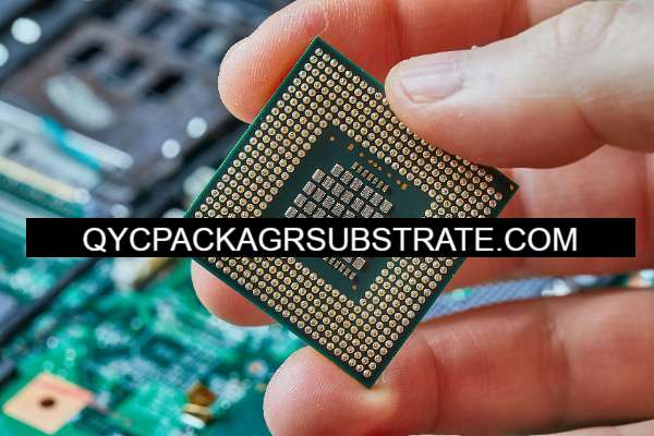
ABF Substrate Firm. Ajinomoto(ABF) and Showa Denko materials are designed for small pitch, high speed and high precision. we QYC has produced 20 layer FC BGA Substrates with high quality.
ABF Substrate (Ajinomoto Build-Up Film Substrate) is a commonly used type of packaging substrate in the semiconductor industry, specifically in the realm of Integrated Circuit (IC) packaging technology. It serves as a crucial component in the assembly of semiconductor devices.
ABF Substrate is not based on colloidal copper foil; instead, it typically involves a build-up process where multiple layers of insulating material and conductive traces are deposited on top of each other to create a multilayer structure. The materials used in ABF substrates are often polymer-based, and the technology is known for its high-density interconnects.
The unique structure of ABF Substrate offers several advantages for IC packaging:
Electrical Properties: ABF Substrate provides excellent electrical properties, including low signal loss and high electrical reliability. This is crucial for ensuring that signals can be transmitted efficiently and accurately within the integrated circuits.
Mechanical Strength: The substrate is designed with durable mechanical properties, capable of withstanding the stresses and strains experienced during both the assembly and utilization of semiconductor devices. This mechanical resilience is essential to guarantee the reliability and longevity of the end product.
High-Density Interconnects: ABF Substrate enables the development of high-density interconnections, enabling the integration of numerous components within a limited space. This is especially vital for contemporary electronic devices, where the emphasis on miniaturization is paramount.
Advanced Solutions: The use of ABF Substrate contributes to the development of more advanced solutions in IC packaging technology. It supports the trend toward smaller and more powerful electronic devices by enabling the fabrication of compact and high-performance semiconductor packages.
While colloidal copper foils are not a typical component of ABF Substrate, the technology does involve the use of conductive materials for creating the interconnects. The specific materials and processes used can vary between manufacturers and depend on the desired characteristics of the final semiconductor package.
Overall, ABF Substrate plays a significant role in advancing IC packaging technology, offering a combination of excellent electrical performance, mechanical strength, and high-density interconnects to meet the demands of modern electronics.
What Functions Does ABF/Ajinomoto Substrate Serve?
ABF (Ajinomoto Build-up Film) substrate is a type of material commonly used in semiconductor packaging. Its unique properties make it suitable for various functions in micro-scale packaging structures. Here are some of the diverse functions that ABF substrate serves:
Electrical Connections: ABF substrate is known for its excellent electrical properties. It provides a reliable and efficient medium for electrical connections between different components in microelectronics devices. The material allows for the creation of intricate wiring patterns, ensuring the proper transmission of electrical signals.
Heat Dissipation: ABF substrates often exhibit good thermal conductivity. This property is crucial for dissipating the heat generated by electronic components during operation. Effective heat dissipation helps maintain the temperature within acceptable limits, preventing overheating and ensuring the reliable performance of the microelectronics.
Mechanical Support: ABF substrates offer mechanical support to the components mounted on them. They provide a stable platform for delicate microelectronics structures, preventing damage from mechanical stress or vibrations. This mechanical support is essential for the longevity and durability of the packaged devices.
High-Performance Packaging: The combination of reliable electrical connections, excellent heat dissipation, and mechanical support makes ABF substrate suitable for high-performance packaging. In applications where advanced functionality and speed are crucial, ABF substrates can contribute to the overall performance of the packaged semiconductor devices.
High-Density Packaging: ABF substrates are often employed in high-density packaging configurations. The material’s properties allow for the creation of compact and tightly integrated electronic devices. This becomes crucial in contemporary electronics, where the emphasis on smaller form factors and enhanced device functionality makes miniaturization and high-density packaging pivotal considerations.
In conclusion, ABF substrate stands out for its ability to offer a blend of electrical, thermal, and mechanical properties, making it highly suitable for advanced microelectronics packaging. Its varied functions collectively enhance the overall dependability, effectiveness, and compact design of electronic devices.
What Are the Different Types of ABF Substrate?
ABF (Ajinomoto Build-up Film) substrates, or more broadly, build-up films, serve as a key component in the production of semiconductor devices and electronic components. They play a vital role in furnishing essential support and connectivity for the diverse components integrated into semiconductor devices. While ABF is a specific type of build-up film, there are variations and types of build-up films used for different applications. Here are some common types:
Standard ABF Substrate:
Design: ABF substrates typically comprise several layers of insulating material and conductive traces, enabling the development of intricate and space-efficient circuitry.
Applications:They find broad application in general semiconductor uses where achieving high-density interconnections and miniaturization is crucial, particularly in advanced integrated circuits (ICs).
High-Frequency ABF Substrate:
Design: This type is specifically designed to support high-frequency applications. The substrate material and design are optimized to minimize signal loss and maintain signal integrity at higher frequencies.
Applications: High-frequency ABF substrates are used in applications like RF (radio frequency) devices, wireless communication modules, and high-speed data transmission.
Thermal ABF Substrate:
Design: Thermal ABF substrates are engineered to have enhanced thermal conductivity and heat dissipation properties. This helps in managing the heat generated by the semiconductor components.
Applications: These substrates find applications in power devices, LEDs (light-emitting diodes), and other components where efficient heat dissipation is critical.
Flexible ABF Substrate:
Design: Flexible ABF substrates are crafted to bend easily and adapt to diverse shapes, typically utilizing flexible materials such as polyimide.
Applications: Flexible ABF substrates find applications in bendable electronic devices, like flexible displays and wearable electronics, where conventional rigid substrates are impractical.
Embedded Component ABF Substrate:
Design: This design enables the integration of passive components, such as resistors and capacitors, directly into the substrate layers, thereby minimizing the overall device footprint.
Applications: Embedded component ABF substrates find utility in scenarios where space is at a premium, emphasizing the critical need to minimize the dimensions of electronic components.
These examples represent only a small sample, and there could be additional specialized ABF substrates tailored for specific applications or industries. The selection of the substrate relies on the needs of the electronic device and its intended use.
How Does ABF/Ajinomoto Substrate Relate to IC Packaging?
ABF (Ajinomoto Build-up Film) substrate plays a crucial role in IC (Integrated Circuit) packaging, and understanding the relationship between the two provides insights into various aspects of chip packaging technology classifications and potential future developments.
Structure and Functionality:
ABF substrate is a type of build-up film that is commonly used as a dielectric material in the packaging of integrated circuits. It is designed to provide electrical insulation and interconnection between different layers of the IC package. The substrate acts as a foundation for mounting and connecting the semiconductor chip within the package.
Applications in Chip Packaging Technology:
ABF substrates are widely used in advanced packaging technologies such as fan-out wafer-level packaging (FO-WLP) and 2.5D/3D packaging. In FO-WLP, ABF is used to create the build-up layers that enable the redistribution of the electrical connections from the chip to the package. This allows for a more compact and efficient packaging of ICs. In 2.5D/3D packaging, ABF substrates are utilized to stack multiple chips vertically, enabling higher performance and integration density.
Classifications and Variations:
The use of ABF substrates contributes to the classification of packaging technologies. Different variations of ABF substrates, with varying thicknesses and material properties, are employed based on the specific requirements of the IC package. The choice of substrate can impact the electrical performance, thermal properties, and overall reliability of the packaged IC.
Potential in Future Developments:
The relationship between ABF substrate and IC packaging is dynamic, with ongoing developments aimed at improving performance, reducing form factor, and enhancing overall efficiency. Innovations in ABF materials, such as the development of low-loss and high-frequency variants, can open up new possibilities for applications in high-performance computing, 5G communications, and other emerging technologies.
Challenges and Considerations:
A deeper investigation into the relationship between ABF substrate and IC packaging should also consider challenges such as thermal management, signal integrity, and reliability. As ICs continue to evolve with increasing complexity and performance demands, addressing these challenges becomes crucial for the successful implementation of ABF substrates in advanced packaging technologies.
In conclusion, ABF substrate is a key element in IC packaging, influencing the design and performance of modern semiconductor devices. Understanding its relationship with IC packaging provides valuable insights into the current state of packaging technologies and points towards potential advancements in the future.
What Sets Ajinomoto Substrate Apart from Traditional PCBs?
By comparing ABF (Ajinomoto Build-up Film) substrate with traditional PCBs, PWBs, motherboards, substrate-like PCBs (SLP), and high-density interconnect (HDI) substrates, we can highlight the unique advantages of ABF substrate in achieving higher performance and more compact packaging.
Material Characteristics: ABF substrate uses Ajinomoto Build-up Film, a high-performance thin film material. Compared to traditional substrate materials, ABF offers better insulation and thermal conductivity, contributing to overall improved performance.
Thinner Packaging: ABF substrate is thinner compared to traditional PCBs and PWBs, allowing for more layers and a more compact design within the same space. This is advantageous for achieving more complex circuit layouts and higher integration in limited spaces.
Higher Density: While HDI and SLP substrates represent high-density interconnects, ABF substrate can further enhance density in some aspects. Its thin film nature allows for smaller via diameters and more compact wiring, accommodating more components on the same-sized substrate.
Excellent Thermal Performance: ABF substrate exhibits excellent thermal conductivity, crucial for handling high-performance chips and circuits. Good thermal conductivity aids in heat dissipation, preventing chip overheating and improving system reliability and stability.
Advanced Manufacturing Technology: ABF substrates typically utilize advanced manufacturing technologies such as laser drilling and fine-line manufacturing. These technologies make it possible to implement complex circuits on small-sized substrates, enhancing manufacturing precision and efficiency.
In summary, ABF substrate, through its superior material characteristics, thinner packaging, higher density, and advanced manufacturing technologies, provides electronic products with higher performance and more compact designs. However, the choice of substrate depends on specific application requirements and manufacturing cost considerations.
What are the Main Structures and Production Technologies of ABF Substrate?
ABF (Ajinomoto Build-up Film) substrate is a high-density interconnect (HDI) substrate employed in semiconductor packaging, essential for establishing electrical connections between integrated circuits (ICs) and printed circuit boards (PCBs). The following provides an in-depth examination of ABF substrate’s primary structures and production methods, encompassing the progression of manufacturing technology and advancements in high-density interconnect manufacturing:
Main Structures of ABF Substrate:
Build-Up Layers: ABF substrates typically feature multiple build-up layers, each comprising conductive traces and insulating dielectric materials. These layers are stacked to form a three-dimensional interconnect structure.
Core Layer: The central layer acts as the substrate’s foundational base, offering mechanical support and commonly crafted from a non-conductive material such as epoxy resin.
Conductive Traces:In each build-up layer, conductive traces link different components and elements within the integrated circuit. These traces are typically made of copper due to its excellent conductivity.
Insulating Dielectric: The spaces between conductive traces are filled with insulating dielectric materials, which prevent short circuits and provide isolation between different circuit elements.
Solder Mask: A protective layer called solder mask is applied over the surface of the substrate to prevent solder bridging and protect the conductive traces from environmental factors.
Production Technologies of ABF Substrate:
Lamination: The manufacturing of ABF substrates includes a lamination procedure, during which various layers of insulating and conductive materials are compressed and solidified to create a stable structure.
Copper Plating: Conductive pathways are formed by copper plating, involving the deposition of a thin copper layer onto the substrate surface.This copper layer is then patterned to form the required circuitry.
Dielectric Layer Formation: Insulating dielectric layers are formed using materials such as epoxy resin or polyimide. These layers are applied through various techniques like spin coating or lamination.
Photolithography: Photolithography is used to define the patterns of conductive traces on the substrate. A photoresist material is applied, exposed to UV light through a mask, and then developed to create the desired circuit pattern.
Drilling and Via Formation: Holes are drilled through the substrate to create vias, which are filled with conductive material to establish vertical connections between different layers.
Evolution of Manufacturing Technology:
The manufacturing technology of ABF substrates has evolved over time, driven by the demand for higher performance and increased miniaturization in electronic devices. Some key trends and advancements include:
Miniaturization: As electronic devices become smaller and more compact, the demand for thinner and more densely packed ABF substrates has increased. Manufacturers have developed advanced techniques to achieve finer features and tighter pitch.
Material Innovations: Ongoing research focuses on developing new materials with improved electrical and thermal properties to enhance the performance of ABF substrates.
Advanced Imaging and Inspection: High-resolution imaging and inspection technologies are employed to ensure the quality and reliability of the intricate circuit patterns on ABF substrates.
3D Integration: The industry is exploring 3D integration techniques, where multiple dies are stacked vertically to increase circuit density and improve overall performance.
Embedded Passive Components: Integration of passive components, such as resistors and capacitors, directly into the substrate is being explored to further reduce the footprint of electronic devices.
In conclusion, the main structures and production technologies of ABF substrate have evolved to meet the demands of modern electronics. Advancements in manufacturing technology, material science, and design techniques continue to drive innovation in the development of high-density interconnect solutions like ABF substrates.
FAQs About ABF(Ajinomoto) Substrate:
What is ABF Substrate?
ABF Substrate is a type of substrate with an anisotropic conductive film, commonly used for micro-connections in electronic devices, facilitating the connection between chips and other components. Its conductivity allows signal transmission both vertically and horizontally.
How does ABF Substrate differ from other connection technologies?
Unlike traditional soldering techniques, ABF Substrate utilizes an anisotropic conductive film for connections, eliminating the need for solder. This connection method is more suitable for miniaturized and lightweight electronic devices, contributing to cost reduction in manufacturing.
What are the main applications of ABF Substrate?
ABF Substrate is primarily used for connecting microchips and other electronic components, widely applied in devices such as smartphones, tablets, and other portable electronic devices.
What are the advantages of ABF Substrate?
The advantages of ABF Substrate include being thin, flexible, lightweight, and relatively cost-effective. As soldering is not required, it also contributes to increased manufacturing efficiency.
What is the manufacturing process of ABF Substrate?
The manufacturing process of ABF Substrate involves placing layers of anisotropic conductive film on the substrate, followed by connecting them to chips or other components through processes like heat pressing. The manufacturing process is relatively simple and suitable for mass production.
How does ABF Substrate perform under temperature variations?
ABF Substrate performs well under a certain range of temperature variations, but extreme temperature conditions may affect its performance. Manufacturers typically provide recommendations regarding the optimal operating temperature range.
Is ABF Substrate reliable?
Under normal operating conditions, ABF Substrate is reliable. However, users should be cautious to avoid excessive bending and extreme conditions to ensure the stability and reliability of the connections.
Can ABF(Ajinomoto) Substrate Lead the Future of IC Packaging?
ABF (Anisotropic Conductive Film) substrate, as a leading technology in IC packaging, indeed has the potential to drive the future development of the modern electronics industry. ABF substrate plays a crucial role in IC packaging, and its unique characteristics make it a powerful technology shaping the future.
ABF substrates excel in thermal conductivity, a crucial factor for dissipating heat in integrated circuits. As electronic devices trend toward greater compactness and higher performance, managing thermal issues becomes increasingly challenging. The notable thermal conductivity of ABF substrates significantly aids in efficient heat dissipation, thereby guaranteeing the stability and reliability of the chips.
Secondly, ABF substrate provides good reliability and stability during the packaging process. This is vital for the lifespan and performance of electronic products. The high-quality manufacturing of ABF substrate and reliable anisotropic conductive adhesive technology help reduce product failure rates, elevating the overall quality.
Additionally, ABF substrate exhibits good electrical performance, contributing to the enhancement of chip performance.This becomes vital in addressing the increasing electronic market demand for devices that are both high-performance and energy-efficient.
In summary, the superior performance of ABF substrate in thermal conductivity, reliability, and electrical properties distinguishes it in the field of IC packaging. As a key technology in the modern electronics industry, ABF substrate is poised to lead the future direction of IC packaging technology, driving innovation and progress in the entire electronic industry.