
Advance Semiconductor substrate supplier, we mainly produce ultra-small bump pitch substrate, ultra-small trace and spacing packaging substrate and Microtrace HDI PCBs.
Within the intricate domain of semiconductor innovation, the Advanced Semiconductor Substrate assumes a prominent role, actively shaping the intricacies of semiconductor devices, from integrated circuits (ICs) to microprocessors. Its influence permeates through the layers of performance, reliability, and functionalities intricately woven within these electronic components. A curated selection of meticulously engineered materials and structures is adeptly calibrated to navigate the dynamic shifts in semiconductor technology.
In the relentless pursuit of more efficient, robust, and compact electronic devices, the rallying cry for innovation within semiconductor substrates echoes resoundingly. Traditional materials, embodied by silicon, grapple with the constraints of scalability and thermal management as technology forges ahead. Consequently, advanced semiconductor substrates now welcome materials like gallium nitride (GaN) and silicon carbide (SiC), each introducing a distinct note to elevate device functionality.
What sets advanced semiconductor substrates apart lies in their remarkable resilience to elevated temperatures, superior electrical performance, and efficient thermal conductivity. These substrates play a pivotal role in crafting the landscape of high-performance electronic devices, extending their influence across diverse industries, including telecommunications, computing, automotive, and aerospace.
Furthermore, the impact of advanced semiconductor substrates resonates into transformative technologies like 5G communication, artificial intelligence, and the Internet of Things (IoT). A steadfast commitment to research and exploration persists, aiming to unveil novel materials and inventive design strategies that consistently push the boundaries of semiconductor technology. This ongoing endeavor ensures that these substrates seamlessly adapt to the ever-evolving demands of the next generation of electronic devices.
Essentially, as the semiconductor industry undergoes perpetual evolution, the development and integration of advanced substrates become pivotal, laying the foundation for heightened performance, superior energy efficiency, and unwavering reliability in electronic systems.
What Marvelous Functions Does Advanced Semiconductor Substrate Possess?
The Advanced Semiconductor Substrate unfolds as a dynamic orchestrator of functions, cementing its crucial role in the ever-evolving landscape of semiconductor devices. Let’s navigate through its distinct features:
Thermal Mastery: At its essence, the substrate excels in orchestrating the dissipation of heat generated during electronic operations. This pivotal function not only prevents overheating issues but also ensures the enduring reliability of electronic devices.
Electrical Finesse: These substrates showcase finesse in electrical performance, facilitating the swift ballet of signal processing and seamless data transmission. This capability is the driving force behind the development of high-speed and high-frequency electronic devices.
Heat-Endurance Virtuoso: A noteworthy characteristic lies in the substrate’s virtuosity to endure higher operating temperatures, a crucial attribute for applications where devices must gracefully navigate demanding thermal environments, such as in automotive and aerospace settings.
Miniaturization Maestro: Assuming a lead role in the ongoing saga of miniaturization, advanced semiconductor substrates empower the creation of devices that are not only smaller but also maintain a crescendo of performance.
Material Symphony: Departing from the conventional, these substrates compose a symphony of materials, including gallium nitride (GaN), silicon carbide (SiC), and other compound semiconductors. This harmonious blend allows for nuanced material selection, tailored to the specific cadence of each application.
Power Electronics Virtuosity: These substrates take center stage in power electronic devices, adeptly handling high voltages and currents while choreographing an elegant dance of thermal management. Their virtuosity is particularly vital in applications like power converters and inverters.
Navigator of Next-Gen Technologies: The advanced features seamlessly align with the demands of next-generation technologies, including 5G communication, artificial intelligence, and the Internet of Things (IoT).
Reliability Ballet: Bolstered by improved materials and innovative choreography, advanced semiconductor substrates perform a reliability ballet, ensuring robust durability and stability for electronic devices across diverse and challenging applications.
In essence, the multifaceted functions of advanced semiconductor substrates compose a symphony of efficient heat dissipation, superior electrical capabilities, resilience to varying temperatures, material adaptability, support for miniaturization, and their pivotal role in steering the course of next-generation technologies. Together, these features establish them as virtuosos shaping the harmonious landscape of high-performance and cutting-edge electronic devices.
Did You Know There Are Various Types of Advanced Semiconductor Substrates?
Let’s reimagine the depiction of advanced semiconductor substrates with a different narrative:
Silicon Renaissance: Silicon, the backbone of semiconductors, undergoes a renaissance, refining its essence with evolved crystal structures and manufacturing techniques. This heralds a new era marked by enhanced performance and adaptability.
Gallium Nitride (GaN) Mastery: GaN takes center stage, showcasing mastery in power electronics and high-frequency applications. Its allure lies in superior electron mobility and adept handling of heightened power densities, reshaping the landscape of semiconductor capabilities.
Silicon Carbide (SiC) Mosaic: SiC emerges as a canvas for innovation, weaving a mosaic of superior thermal conductivity and a wide bandgap. Its intricate patterns define applications demanding resilience in high-power environments, such as power electronics and RF devices.
Sapphire Radiance: Sapphire steps into the semiconductor realm with radiance, contributing to the brilliance of LEDs and the precision of RFICs. It adds a touch of sophistication to electronic illumination, painting a vivid picture of technological advancement.
Aluminum Nitride (AlN) Harmony: AlN orchestrates a harmonious blend, celebrated for its high thermal conductivity. Its balanced notes resonate in applications where efficient heat dissipation is crucial, particularly in the realm of high-power electronic devices.
Glass Choreography: Glass takes center stage in an elegant choreography, serving as a flexible substrate for the rhythmic dance of electronics and displays. Its transparent, flexible, and smooth movements create a visual and tactile masterpiece, particularly in the domain of flexible OLED displays.
Germanium (Ge) Sonata: Germanium serenades us with its role in orchestrating photodetectors and infrared sensors, adding a melodic touch to optical and sensing applications. Its nuanced notes resonate with precision and clarity in the symphony of semiconductor innovation.
These substrates, akin to characters in a dynamic narrative, play distinctive roles, shaping the plot of semiconductor technology. The selection of a specific substrate becomes a carefully composed piece, considering the interplay of factors such as application, electrical properties, thermal requirements, and the unfolding chapters of manufacturing intricacies. The ongoing storyline of research and development continues to unveil new materials and substrates, propelling semiconductor technology into uncharted and exciting territories.
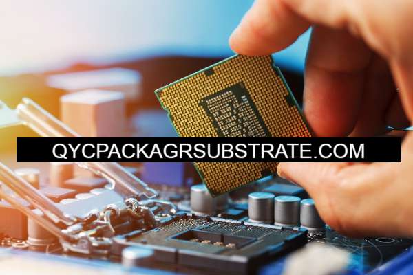
What’s the Relationship Between Advanced Semiconductor Substrate and IC Packaging?
The interplay between advanced semiconductor substrates and integrated circuit (IC) packaging is a dynamic and symbiotic relationship, deeply embedded in the intricacies of electronic device development. Let’s explore this connection through a different lens:
Foundational Nexus: Advanced semiconductor substrates serve as the bedrock upon which the intricate layers of semiconductor materials are meticulously crafted, providing the elemental canvas for the creation of integrated circuits (ICs).
Conductivity Hub: Functioning as more than just a passive layer, the semiconductor substrate actively facilitates electrical connectivity within the IC. The choice of substrate material significantly influences electrical performance, impacting signal speed, power efficiency, and overall circuit behavior.
Thermal Symphony: Playing a pivotal role in thermal management, these substrates conduct the symphony of heat dissipation, preventing overheating and safeguarding the reliability of ICs during operation.
Pioneering Miniaturization: The characteristics of advanced substrates contribute to the ongoing saga of miniaturization. A substrate conducive to high integration and packaging density is akin to a key protagonist, enabling the creation of smaller, yet more powerful, electronic devices.
Synergy with Packaging Technologies: The substrate harmonizes with various packaging technologies, ensuring compatibility with methods like flip-chip or wire bonding. This synergy is vital for seamless integration during the packaging process.
Intricate Interconnection: The substrate intricately weaves its connectivity with the IC package, forming a complex network through wire bonds, solder balls, or other interconnection methods. This web of connections facilitates the seamless transmission of signals between the IC and its external environment.
Guardian and Encasement: The IC packaging takes on the role of a protective guardian, encasing the semiconductor substrate and its integrated components. It shields the delicate semiconductor layers from external factors, ensuring durability, and safeguarding against environmental stressors.
In essence, the relationship between advanced semiconductor substrates and IC packaging is akin to a symbiotic dance. The substrate sets the stage, influencing electrical properties and thermal dynamics, while packaging encapsulates and shields, ensuring the resilience and longevity of the semiconductor device. Together, they form a collaborative duet, propelling advancements in electronic devices in terms of performance, size, and reliability.
How Does Advanced Semiconductor Substrate Differ from Traditional PCBs?
Let’s explore the distinctions between advanced semiconductor substrates and traditional printed circuit boards (PCBs) using a different narrative, accentuating their unique attributes in materials, functionalities, and application domains:
Material Alchemy:
Advanced Semiconductor Substrates: Embarking on a journey of material alchemy, these substrates weave a tale with silicon, gallium nitride (GaN), and silicon carbide (SiC). Selected for their specialized properties, these materials form a canvas for crafting high-performance applications.
Traditional PCBs: In contrast, traditional PCBs embrace a more commonplace alchemy, employing materials like fiberglass-reinforced epoxy laminates. While practical, they may lack the intricacies found in the material composition of semiconductor substrates.
Functional Choreography:
Advanced Semiconductor Substrates: Unfolding as a dynamic stage for semiconductor devices, these substrates host a choreography of intricate electronic components, orchestrating performances in realms of high-speed, high-frequency, and power electronics.
Traditional PCBs: Serving as the foundational scaffold for electronic components, traditional PCBs engage in a versatile dance of interconnections, providing structural support for electronic devices. Yet, their performance may not attain the same crescendo as advanced semiconductor substrates.
Integration Symphony:
Advanced Semiconductor Substrates: Orchestrated for seamless integration and miniaturization, these substrates lead the symphony toward compact and potent electronic devices, embodying the nuanced movements of modern technology.
Traditional PCBs: While integral in connecting components, traditional PCBs may not sway with the same emphasis on miniaturization. They harmonize in the ensemble, accommodating diverse components in a cost-effective orchestration.
Electrical Harmony:
Advanced Semiconductor Substrates: Crafted for a virtuoso electrical performance, these substrates showcase attributes like high electron mobility, minimal signal loss, and adept thermal conductivity. They take center stage in applications demanding a harmonious blend of top-tier performance.
Traditional PCBs: Designed for reliable electrical connections, traditional PCBs contribute to the harmonics of general electronic applications. However, their performance may not reach the same zenith as advanced semiconductor substrates.
Application Narrative:
Advanced Semiconductor Substrates: Play pivotal roles in the narrative of cutting-edge technologies like 5G communication, high-power electronics, and advanced sensors. They shine in fields where enhanced electrical and thermal properties take the spotlight.
Traditional PCBs: Woven into the storyline of various electronic devices, from consumer electronics to industrial equipment, traditional PCBs showcase their versatility across a broad spectrum of applications.
In essence, the intricate tale of advanced semiconductor substrates and traditional PCBs unfolds as a multi-dimensional performance. While advanced substrates take the lead in high-performance realms, traditional PCBs contribute to the versatile orchestration of electronic devices, each playing a vital role in the grand production of modern technology.
FAQs AboutAdvance Semiconductor substrate
What characterizes an advanced semiconductor substrate?
An advanced semiconductor substrate is a specialized material meticulously designed for crafting semiconductor devices. This category encompasses materials such as silicon, gallium nitride (GaN), silicon carbide (SiC), sapphire, and aluminum nitride (AlN), each selected for its unique properties.
How does an advanced semiconductor substrate distinguish itself from traditional PCBs?
Unlike traditional Printed Circuit Boards (PCBs), advanced semiconductor substrates serve as the fundamental canvas for semiconductor devices, boasting superior thermal conductivity, electrical performance, and tailored material properties for high-performance applications.
What are the fundamental structures and manufacturing technologies of advanced semiconductor substrates?
Structures and manufacturing technologies vary depending on the substrate material. Silicon substrates may involve methods like Czochralski or Float Zone, while GaN substrates could utilize hydride vapor phase epitaxy (HVPE) or metal-organic chemical vapor deposition (MOCVD). Silicon carbide (SiC) substrates might employ techniques such as physical vapor transport (PVT) or chemical vapor deposition (CVD).
In which applications are advanced semiconductor substrates commonly applied?
Advanced semiconductor substrates play a vital role in diverse industries, including electronics, telecommunications, power electronics, and lighting. Their significance lies in the development of high-performance devices such as power amplifiers, LEDs, and RF (radio frequency) components.
How does the choice of substrate material impact the performance of semiconductor devices?
The choice of substrate material significantly influences the electrical, thermal, and mechanical properties of semiconductor devices. Silicon is widely adopted for its mature manufacturing processes, while GaN and SiC are favored for applications requiring high-power capabilities.
Are there distinct types of advanced semiconductor substrates?
Absolutely, a diverse array of advanced semiconductor substrates exists, each showcasing unique properties. Common types encompass silicon, gallium nitride (GaN), silicon carbide (SiC), sapphire, and aluminum nitride (AlN). These substrates cater to different needs in terms of performance, power handling, and frequency range.
What role do advanced semiconductor substrates play in IC packaging?
Advanced semiconductor substrates play a pivotal role in the packaging of integrated circuits (ICs). The choice of substrate material significantly impacts the thermal performance, electrical connectivity, and overall reliability of the packaged IC.
Can you elucidate the key differences between silicon, GaN, and SiC substrates?
Silicon, with its mature manufacturing processes, contrasts with GaN and SiC, offering advantages in high-power and high-frequency applications. GaN is recognized for its wide bandgap and high electron mobility, while SiC exhibits excellent thermal conductivity and hardness.
What are the manufacturing processes involved in advanced semiconductor substrates?
Manufacturing processes vary depending on the substrate material. Common techniques include crystal growth methods like Czochralski (Cz), Float Zone (FZ), or vapor phase epitaxy (VPE). Subsequent processes may encompass polishing, doping, and lithography to achieve the desired substrate properties.
What trends are emerging in the realm of advanced semiconductor substrates?
Emerging trends include the development of new substrate materials, advancements in manufacturing processes for enhanced performance, and the integration of substrates into advanced packaging technologies. Ongoing research aims to elevate the efficiency and capabilities of substrates for next-generation semiconductor devices.
In Conclusion
In conclusion, the domain of advanced semiconductor substrates unfolds as a captivating narrative, weaving together materials, technologies, and applications. From the stalwart silicon to the dynamic gallium nitride (GaN) and silicon carbide (SiC), these substrates take center stage in shaping high-performance semiconductor devices across diverse industries.
The choice of substrate material emerges as a linchpin, influencing the intricate dance of electrical, thermal, and mechanical characteristics in semiconductor devices. Silicon, with its seasoned manufacturing processes, shares the limelight with the agile GaN and robust SiC, each contributing a unique flair to the technological panorama.
The manufacturing odyssey of these substrates involves a choreography of processes, including the elegance of Czochralski, the precision of Float Zone, and the artistry of vapor phase epitaxy. The integration of advanced semiconductor substrates into the grand production of integrated circuits (ICs) underscores their importance, shaping thermal performance, electrical connectivity, and overall reliability.
Looking forward, the landscape of advanced semiconductor substrates unfolds with emerging trends, featuring the genesis of novel substrate materials, the evolution of manufacturing techniques, and the seamless fusion of substrates with avant-garde packaging technologies. Ongoing research endeavors paint a canvas of a future where these substrates will continue to elevate the efficiency and capabilities of next-generation semiconductor devices. In this ever-evolving symphony of technology and innovation, advanced semiconductor substrates stand as both the canvas and conductor for the future of electronics.