
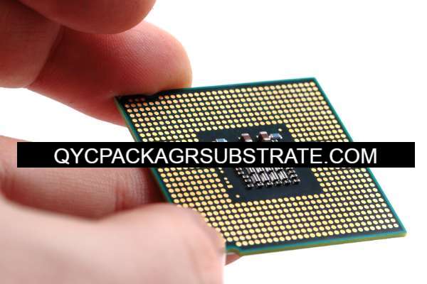
Advance Semiconductor substrate Vender. High speed and high frequency material packaging substrate manufacturing. Advanced packaging substrate production process and technology.
When we dive into the domain of state-of-the-art semiconductor substrates, we’re essentially exploring the foundational materials that serve as the backbone for electronic marvels in semiconductor manufacturing. Historically, silicon wafers have been the stalwarts in this arena. These wafers undergo a series of intricate processes, from deposition to etching and doping, birthing the complexities of integrated circuits and diverse electronic components.
The trajectory of advancing semiconductor technology often entails a choreography of refinements in the materials, processes, and designs of these substrates. Let’s stroll through a few instances:
Silicon-On-Insulator (SOI): Envision this as the virtuoso enhancing semiconductor device performance by delicately layering a wispy sheet of silicon atop an insulating material. SOI is the maestro orchestrating a reduction in power consumption and a symphony amplification in the speed of integrated circuits.
III-V Semiconductors: Bid farewell to the era of traditional silicon-based semiconductors; compounds dabbling in the elements from groups III and V of the periodic table (think gallium arsenide, indium phosphide) are stepping into the spotlight or undergoing a sartorial transformation. These materials might just steal the limelight in specific applications.
2D Materials: Enter the avant-garde with graphene and transition metal dichalcogenides (TMDs) – these are the rebels of advanced substrates, flaunting a distinctive electronic panache. Slim and armed with captivating electrical and thermal characteristics, they’re the outliers in the semiconductor narrative.
Advanced Packaging Technologies: While not hogging the limelight as substrates per se, the evolution of packaging technologies – the 3D packaging, chip stacking, and the fusion of heterogeneous integration – can throw a grand soirée, significantly influencing the performance and functionalities of semiconductor devices.
What Functions do Advanced Semiconductor Substrates Serve?
Diving into the intricate world of advanced semiconductor substrates unveils a transformative narrative in electronic device manufacturing. These substrates, crafted with avant-garde materials and technologies, don the mantle of architects, orchestrating a symphony of enhanced performance, efficiency, and capabilities:
Electrical Symphony Conductors: At the core of their mission is the artistry of elevating the electrical performance of electronic devices. Picture these substrates as maestros, enhancing carrier mobility, orchestrating a reduction in power consumption, and infusing a rhythm of speed into integrated circuits.
Power Efficiency Virtuosos: Enter the stage where certain substrates, notably the Silicon-On-Insulator (SOI) virtuosos, take the spotlight. Their act involves the finesse of minimizing power leakage, a crucial performance for devices relying on batteries and applications demanding judicious power consumption.
Thermal Ballet Choreographers: Among their standout performances is the mastery of thermal conductivity, especially in substrates housing 2D materials. These substrates are the choreographers, gracefully dissipating heat during device operation, avoiding the pitfalls of overheating, and maintaining an optimal functional tempo.
Miniaturization and Integration Pioneers: Picture a synchronized dance of electronic components becoming smaller and more densely packed. These substrates are the pioneers, enabling the industry’s dance towards miniaturization and seamlessly integrating more functionality into confined spaces.
Signal Integrity Artists: Armed with improved materials and designs, these substrates step onto the canvas of signal integrity optimization. They’re the artists who minimize signal losses, quell crosstalk, and create a harmonious environment for reliable communication and high-speed data transmission.
Heterogeneous Integration Trailblazers: These substrates assume the role of trailblazers in the theater of heterogeneous integration. They set the stage for a diverse cast of materials and technologies to coexist on a single chip, fostering a narrative where digital and analog components seamlessly share the spotlight.
Materials Evolution Hosts: Embracing the winds of technological change, these substrates open their doors to new materials beyond the conventional silicon. Imagine III-V semiconductors and 2D materials like graphene taking center stage, allowing for the exploration of novel electronic properties and performance enhancements.
Champions of Packaging Innovation: While not stealing the limelight as substrates per se, their influence extends to the realm of packaging technologies. The rise of 3D packaging and chip stacking is their legacy, significantly influencing device performance and shaping innovative form factors.
In essence, advanced semiconductor substrates emerge as the unsung conductors, shaping the symphony of innovation in electronic devices. Their evolution is a dynamic force, propelling progress in performance, energy efficiency, thermal regulation, and the grand tapestry of functionality. They are the architects sculpting the destiny of contemporary electronics and standing at the forefront of emerging technologies.
What Types of Advanced Semiconductor Substrate Exist?
Embarking on an intriguing journey into the realm of advanced semiconductor substrates propels us into a sphere where technological innovation claims the spotlight. Each meticulously crafted substrate, employing cutting-edge materials and sophisticated technologies, plays a unique role in elevating the performance, efficiency, and adaptability of semiconductor devices. Let’s delve into the diverse categories:
Silicon-On-Insulator (SOI): Envision a delicate performance, where a slim layer of silicon gracefully leads atop an insulating material like silicon dioxide. SOI emerges as a luminary, adeptly reducing power consumption, enhancing performance, and orchestrating a ballet of heightened transistor speed.
III-V Semiconductors: Enter the domain of compounds resulting from the alchemical fusion of elements from groups III and V of the periodic table, exemplified by gallium arsenide (GaAs) or indium phosphide (InP). These semiconductor maestros, akin to virtuosic performers, demonstrate superior electron mobility, propelling them to the forefront of high-frequency and high-speed applications.
2D Materials: Immerse yourself in substrates woven with the finesse of two-dimensional materials like graphene or transition metal dichalcogenides (TMDs). These substrates become canvases where unique electronic properties, including high electron mobility and exceptional thermal conductivity, paint a portrait of improved device performance.
Gallium Nitride (GaN) Substrates: Picture a powerhouse in the realm of power electronics and high-frequency devices. GaN substrates take center stage with attributes like a high breakdown voltage, a wide bandgap, and stellar electron mobility, conducting a symphony for power amplifiers and LEDs.
Germanium-on-Insulator (GeOI): A sibling to SOI but with a twist – visualize germanium stepping into the limelight as the slim top layer on an insulating substrate. Germanium, with its distinct electrical properties, assumes a lead role in the saga of advanced transistors.
Diamond Substrates: Envision the rising star in the substrate ensemble, diamond, flaunting exceptional thermal conductivity and a wide bandgap. Diamond substrates take center stage, demonstrating prowess in handling high power densities, a virtuoso act for high-power electronic devices.
Compound Semiconductor Substrates: Envision substrates forged through the fusion of silicon carbide (SiC) or gallium nitride (GaN), a process akin to a technological alchemy. Crafted by the artistry of compound semiconductors, these substrates proudly showcase benefits such as the capability for high-temperature operation, an increased breakdown voltage, and exceptional thermal conductivity.
Flexible Substrates: Step into the domain of flexibility, where substrates meticulously crafted from pliable materials, often polymers, engage in a graceful ballet. These substrates serve as the canvas for applications such as flexible displays, wearable electronics, and the artistic integration of flexible electronic components.
Organic Substrates: Envision a narrative where organic materials take center stage, shaping the storyline of organic electronics. Characterized by their lightweight and cost-effectiveness, organic substrates play a pivotal role in applications like organic light-emitting diodes (OLEDs) and the poetic choreography of organic photovoltaics.
Advanced Packaging Substrates: While not seizing the limelight, picture advancements in packaging technologies featuring silicon interposers or through-silicon vias (TSVs). They contribute significantly to the ensemble, playing a vital role in the overall performance and the intricate dance of miniaturizing electronic devices.
This diverse assembly of advanced semiconductor substrates unfolds a tale of innovation, perpetually adapting to the dynamic needs of emerging technologies and the ever-evolving landscape of cutting-edge electronic devices.
How Does Advanced Semiconductor Substrate Differ from Traditional PCBs?
Embarking on an exploration of advanced semiconductor substrates versus traditional Printed Circuit Boards (PCBs) necessitates a nuanced examination of materials, design intricacies, and performance attributes. Let’s reframe these distinctions with a fresh perspective:
Material Composition:
Traditional PCBs: Forged from rigid materials like fiberglass-reinforced epoxy laminates (FR-4), providing stability but limiting flexibility.
Advanced Semiconductor Substrates: Embrace a diverse array of materials—silicon, silicon carbide (SiC), gallium nitride (GaN), and other sophisticated compounds. These materials are meticulously selected for their specific electrical, thermal, and mechanical properties, contributing to an elevated level of performance.
Flexibility:
Traditional PCBs: Predominantly rigid, constraining applications in scenarios requiring flexibility.
Advanced Semiconductor Substrates: Certain substrates, such as their flexible or organic counterparts, gracefully adapt to various shapes, finding relevance in applications such as wearable electronics and flexible displays.
Applications:
Traditional PCBs: Pervasive in everyday electronic devices, seamlessly integrating into scenarios where rigidity is acceptable, such as computers, smartphones, and household electronics.
Advanced Semiconductor Substrates: Tailored for high-performance applications where specific electrical properties or environmental conditions are pivotal. Examples include power electronics, high-frequency devices, and advanced sensors.
Complexity:
Traditional PCBs: Characterized by simpler designs, tailored for standard electronic circuits with moderate complexity.
Advanced Semiconductor Substrates: Accommodate highly intricate and integrated circuits, leveraging advanced materials to enhance functionality.
Thermal Performance:
Traditional PCBs: Constrained by limited thermal conductivity, grappling with challenges in applications demanding efficient heat dissipation.
Advanced Semiconductor Substrates: Engineered with materials boasting superior thermal conductivity—a critical feature for effective heat management in high-power electronic devices.
Cost:
Traditional PCBs: Generally more economically viable due to commonplace materials and straightforward manufacturing processes.
Advanced Semiconductor Substrates: May incur higher costs owing to the utilization of specialized materials and advanced manufacturing techniques.
Performance Metrics:
Traditional PCBs: Well-suited for standard applications with moderate performance requirements.
Advanced Semiconductor Substrates: Tailored for high-performance demands, delivering amplified speed, power efficiency, and advanced capabilities.
In essence, while traditional PCBs seamlessly integrate into everyday electronics, advanced semiconductor substrates cater to specialized applications requiring superior performance, flexibility, and specific material attributes. The choice between them pivots on the unique requirements of the electronic system or device in question.
What Sets Apart Advanced Semiconductor Substrate from Traditional PCBs?
Navigating the distinctions between advanced semiconductor substrates and traditional Printed Circuit Boards (PCBs) unveils a mosaic of differences in material composition, design intricacies, flexibility, and performance benchmarks:
Material Composition:
Traditional PCBs:Forged from durable materials like fiberglass-reinforced epoxy laminates (FR-4), these substrates provide a foundation of stability, albeit with inherent constraints on flexibility.
Advanced Semiconductor Substrates: Embracing a varied spectrum of materials, including silicon, silicon carbide (SiC), gallium nitride (GaN), and other intricate compounds, signifies a thoughtful selection process. These materials are chosen with precision to cater to distinct electrical, thermal, and mechanical properties, thereby enhancing overall performance.
Flexibility:
Traditional PCBs: Predominantly rigid, constraining applications in scenarios necessitating flexibility.
Advanced Semiconductor Substrates: Certain variants, such as flexible or organic substrates, showcase a graceful adaptability to various shapes, playing pivotal roles in applications like wearable electronics and flexible displays.
Applications:
Traditional PCBs: Widespread in daily electronic companions, effortlessly assimilating into environments where sturdiness is embraced, including computers, smartphones, and household electronics.
Advanced Semiconductor Substrates: Tailored for high-performance applications where specific electrical properties or environmental conditions are paramount. Examples include power electronics, high-frequency devices, and advanced sensors.
Complexity:
Traditional PCBs: Characterized by simpler designs, tailored for standard electronic circuits with moderate complexity.
Advanced Semiconductor Substrates: Accommodate highly intricate and integrated circuits, leveraging advanced materials to enhance functionality.
Thermal Performance:
Traditional PCBs: Constrained by limited thermal conductivity, grappling with challenges in applications demanding efficient heat dissipation.
Advanced Semiconductor Substrates: Engineered with materials boasting superior thermal conductivity, a critical feature for effective heat management in high-power electronic devices.
Cost:
Traditional PCBs: Generally more economically viable due to commonplace materials and straightforward manufacturing processes.
Advanced Semiconductor Substrates: May incur higher costs owing to the utilization of specialized materials and advanced manufacturing techniques.
Performance Metrics:
Traditional PCBs: Well-suited for standard applications with moderate performance requirements.
Advanced Semiconductor Substrates: Tailored for high-performance demands, delivering amplified speed, power efficiency, and advanced capabilities.
In essence, traditional PCBs seamlessly integrate into everyday electronics, while advanced semiconductor substrates cater to specialized applications requiring superior performance, flexibility, and specific material attributes. The choice between them pivots on the unique requirements of the electronic system or device in question.