
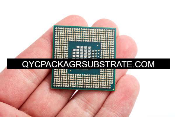
Advanced Flip Chip Substrates Manufacturer
Advanced Flip Chip Substrates Manufacturer,Advanced Flip Chip Substrates are high-performance platforms designed for mounting flip chip integrated circuits. These substrates feature a sophisticated layout with fine-pitch bumps or pads for direct connection to the chip’s I/O pads, enabling high-density packaging and enhanced electrical performance. Typically made from materials such as FR-4, BT resin, or high-frequency laminates, advanced flip chip substrates offer excellent thermal and electrical conductivity. They are crucial for applications requiring high-speed data transmission and reliability, including in consumer electronics, automotive systems, and high-performance computing. Their advanced design ensures robust signal integrity and efficient heat dissipation, meeting the demands of cutting-edge technology.
What is an Advanced Flip Chip Substrate?
An Advanced Flip Chip Substrate is a sophisticated type of substrate used in semiconductor packaging to support flip chip technology. Flip chip technology involves flipping the semiconductor die so that its active side faces downward, with connections made through solder bumps directly to the substrate. This approach offers several advantages over traditional wire bonding, including improved electrical performance, reduced inductance, and enhanced thermal dissipation.
An Advanced Flip Chip Substrate typically features a high-density interconnect structure, which allows for a large number of connections in a compact area. This is achieved through the use of fine-pitch pads and microvias, which are small, high-precision holes filled with conductive material to connect different layers of the substrate. These substrates are often made from high-performance materials such as advanced epoxy resins, ceramics, or metalized ceramics, providing excellent thermal and electrical properties.
The design of an Advanced Flip Chip Substrate must accommodate various factors, including thermal expansion, mechanical stress, and electrical signal integrity. Advanced substrates often incorporate multiple layers, including high-density interconnects (HDI), to support complex integrated circuits (ICs) and enhance overall performance.
Overall, Advanced Flip Chip Substrates are crucial in modern electronics, enabling the development of smaller, faster, and more reliable electronic devices. They are widely used in high-performance applications such as processors, memory modules, and communication devices, where space and performance constraints are critical.
Advanced Flip Chip Substrates Manufacturer
What are the Design Guidelines for Advanced Flip Chip Substrates?
Designing Advanced Flip Chip Substrates requires careful consideration of several factors to ensure optimal performance, reliability, and manufacturability. Here are some key design guidelines:
- Thermal Management: Effective heat dissipation is critical. Ensure that the substrate design includes sufficient thermal vias or heat spreaders to manage heat generated by the die. Consider the use of thermal interface materials and heat sinks if necessary.
- Electrical Performance: Minimize electrical resistance and inductance by using high-quality conductors and optimizing trace routing. Implementing fine-pitch pads and using high-density interconnect (HDI) technologies can improve signal integrity and reduce noise.
- Mechanical Stability:Ensure that the substrate provides adequate mechanical support to prevent warping or deformation. This is particularly important for high-density designs where precise alignment is crucial. Use materials with appropriate thermal expansion coefficients to match those of the die and other components.
- Layer Stack-up: Carefully design the layer stack-up to balance performance and manufacturability. Incorporate sufficient layers for signal routing, power distribution, and ground planes. Consider the use of multiple dielectric layers to enhance electrical isolation and reduce crosstalk.
- Via Design: Use microvias and blind/buried vias appropriately to connect different layers. Ensure vias are placed to minimize signal degradation and optimize electrical performance. Avoid placing vias in high-current paths unless they are properly designed to handle the current.
- Pad and Bump Design:Optimize pad size and bump spacing to match the flip chip die. Ensure that the bump size and pitch are compatible with the soldering process and that they provide reliable electrical connections.
- Manufacturability:Design the substrate with manufacturing constraints in mind. This includes considerations for photolithography, etching, and plating processes. Avoid overly complex designs that may be challenging or costly to produce.
- Testing and Reliability: Incorporate test pads and other features that facilitate the testing of the final assembly. Design the substrate to withstand environmental stresses such as temperature variations, humidity, and mechanical shocks.
- Material Selection: Choose high-performance materials that meet the requirements for thermal conductivity, dielectric strength, and mechanical properties. Common materials include FR-4, high-frequency laminates, and advanced ceramics.
By following these guidelines, you can design Advanced Flip Chip Substrates that meet the demands of high-performance electronic applications, ensuring reliability and efficiency in the final product.
What is the Fabrication Process for Advanced Flip Chip Substrates?
The fabrication process for Advanced Flip Chip Substrates involves several complex and precise steps to ensure high performance and reliability. Here’s an overview of the key stages in the process:
- Design and Layout: The process begins with the design phase, where the substrate layout is created using CAD tools. This includes defining the layer stack-up, pad and via placements, and routing for signal, power, and ground connections.
- Material Selection: Appropriate materials are selected based on the performance requirements of the substrate. Common materials include high-performance epoxy resins, ceramics, and metalized ceramics. The choice of materials impacts thermal management, electrical performance, and mechanical stability.
- Layer Preparation:The substrate is built up in multiple layers. Each layer is prepared separately, typically starting with a base material such as a copper-clad laminate. The copper layers will be patterned to create the circuit traces and pads.
- Photolithography: A photosensitive film or dry film is applied to the copper layers. This film is then exposed to UV light through a mask that defines the circuit patterns. The exposed film is developed to reveal the underlying copper areas that will be etched away.
- Etching: The exposed copper areas are etched away using chemical solutions, leaving behind the desired circuit patterns. This process creates the conductive paths required for the flip chip connections.
- Via Formation: Vias (holes that connect different layers) are drilled or laser-ablated through the substrate. These vias are then plated with metal to create conductive paths between layers. For high-density designs, microvias or blind/buried vias are often used.
- Layer Alignment and Bonding: The layers are aligned and bonded together using adhesive or laminate materials. This step involves precise alignment to ensure that all vias and pads are properly connected across layers.
- Copper Plating and Surface Finish: Additional copper is plated onto the surface and within vias to ensure adequate conductivity and to form the pad structures. A surface finish, such as electroless nickel immersion gold (ENIG) or immersion silver, is applied to protect the copper and enhance solderability.
- Solder Bump Formation: Solder bumps are applied to the pad areas where the flip chip die will make contact. This is typically done using a stencil and solder paste or by electroplating solder onto the pads.
- Inspection and Testing: The fabricated substrates undergo rigorous inspection and testing to verify the integrity of the circuitry, vias, and solder bumps. This includes electrical testing, visual inspection, and sometimes X-ray analysis to check for hidden defects.
- Final Processing: Any final processing steps, such as trimming, routing, or adding additional features, are completed. The substrates are then cleaned and prepared for assembly with the flip chip die.
- Assembly: The flip chip die is attached to the substrate using the solder bumps, and the assembly is subjected to reflow soldering to create the final electrical connections. The assembled substrates are then tested to ensure that the flip chip connections are reliable and functioning correctly.
Each step in the fabrication process must be carefully controlled to ensure that the Advanced Flip Chip Substrate meets the stringent requirements of high-performance electronic applications.
How Do You Manufacture Advanced Flip Chip Substrates?
Manufacturing Advanced Flip Chip Substrates involves a series of precise and carefully controlled steps to ensure high quality and performance. Here’s a detailed overview of the manufacturing process:
- Design and Layout:The process starts with creating a detailed design using CAD software. This design includes the substrate’s layer stack-up, pad and via placements, and routing for electrical connections. The design must meet the specifications for electrical performance, thermal management, and mechanical stability.
- Material Selection: High-performance materials are selected based on the requirements of the substrate. Common choices include advanced epoxy resins, high-frequency laminates, and metalized ceramics. These materials are chosen for their thermal conductivity, electrical insulation, and mechanical properties.
- Layer Preparation: The substrate is built up in multiple layers. Each layer typically begins with a copper-clad laminate. The copper layers are patterned using photolithography to define circuit traces and pads.
- Photolithography: A photosensitive film or dry film is applied to the copper layers. This film is exposed to UV light through a mask that defines the circuit patterns. The exposed film is developed, leaving a protective layer over the copper areas that are not to be etched away.
- Etching: The exposed copper areas are etched away using chemical solutions, leaving behind the circuit patterns. This step creates the conductive paths necessary for the flip chip connections.
- Via Formation: Vias (holes that connect different layers) are drilled or laser-ablated through the substrate. These vias are then plated with metal to create conductive paths between layers. Microvias or blind/buried vias may be used for high-density designs.
- Layer Alignment and Bonding: The layers are precisely aligned and bonded together using adhesive or laminatematerials. Proper alignment is crucial to ensure that all vias and pads are correctly interconnected across layers.
- Copper Plating and Surface Finish: Additional copper is plated onto the surface and within vias to enhance conductivity and form the pad structures. A surface finish, such as electroless nickel immersion gold (ENIG) or immersion silver, is applied to protect the copper and improve solderability.
- Solder Bump Formation: Solder bumps are created on the pad areas where the flip chip die will make contact. This can be done using a stencil and solder paste or by electroplating solder onto the pads.
- Inspection and Testing: The substrates undergo thorough inspection and testing to verify the integrity of the circuitry, vias, and solder bumps. This includes electrical testing, visual inspection, and sometimes X-ray analysis to detect hidden defects.
- Final Processing: Any additional processing steps, such as trimming, routing, or adding extra features, are completed. The substrates are then cleaned to remove any contaminants or residues.
- Assembly: The flip chip die is attached to the substrate using the solder bumps. The assembly undergoes reflow soldering to create the final electrical connections. Post-assembly testing ensures the connections are reliable and that the substrate meets performance specifications.
Each stage of the manufacturing process is carefully controlled to produce Advanced Flip Chip Substrates that meet the high standards required for modern electronic applications. Quality assurance throughout the process is critical to ensure the final product performs reliably in its intended application.
How Much Should Advanced Flip Chip Substrates Cost?
The cost of Advanced Flip Chip Substrates can vary significantly based on several factors. Here’s an overview of the key elements that influence pricing:
- Material Costs: The choice of materials impacts the overall cost. High-performance materials like advanced epoxy resins, high-frequency laminates, and metalized ceramics can be expensive. Specialized materials for thermal management and electrical performance can also add to the cost.
- Complexity and Design: The complexity of the substrate design plays a major role in cost. Advanced Flip Chip Substrates with high-density interconnects (HDI), multiple layers, fine-pitch pads, and microvias require more intricate manufacturing processes and higher precision, which can increase costs.
- Layer Count: Substrates with more layers typically cost more due to the additional processing steps and materials required. Each layer needs to be aligned and bonded accurately, which adds to the complexity and cost.
- Via Technology: The use of advanced via technologies such as microvias or blind/buried vias adds to the manufacturing cost. These technologies require specialized equipment and processes, contributing to higher expenses.
- Production Volume: Economies of scale play a significant role in pricing. Higher production volumes can lower the cost per unit due to reduced setup and material costs. Conversely, smaller production runs or custom designs generally result in higher per-unit costs.
- Fabrication Process: The complexity of the fabrication process, including photolithography, etching, plating, and solder bump formation, affects the overall cost. Advanced processes and equipment required for high-precision manufacturing can drive up prices.
- Testing and Quality Assurance: Extensive testing and quality assurance procedures add to the cost. Rigorous inspection, electrical testing, and reliability testing ensure that the substrates meet performance and quality standards.
- Additional Features: Any extra features such as custom thermal management solutions, enhanced surface finishes, or specific packaging requirements can increase the cost.
As a rough estimate, the cost of Advanced Flip Chip Substrates can range from $10 to $100 per unit or more, depending on the factors mentioned above. For high-volume production, the cost per unit tends to decrease, while for low-volume or highly customized designs, the cost can be significantly higher.
For precise pricing, it is advisable to consult with substrate manufacturers or suppliers, providing detailed specifications and requirements to obtain accurate quotes tailored to specific needs.
What is the Base Material for Advanced Flip Chip Substrates?
The base material for Advanced Flip Chip Substrates is a critical factor in determining the substrate’s overall performance, reliability, and suitability for various applications. Here’s an overview of common base materials used:
- Epoxy Resin (FR-4): Epoxy resin is one of the most widely used base materials for printed circuit boards (PCBs), including advanced flip chip substrates. FR-4 is a glass-reinforced epoxy laminate that provides good electrical insulation, mechanical strength, and thermal stability. While it is suitable for many applications, high-frequency and high-performance designs may require more specialized materials.
- High-Frequency Laminates: For applications that involve high-frequency signals, such as RF and microwave communications, specialized high-frequency laminates are used. These materials, such as Rogers or Taconic laminates, offer low dielectric loss, stable electrical properties over a wide frequency range, and good thermal performance. They are ideal for substrates requiring precise signal integrity.
- Ceramic Substrates: Advanced flip chip substrates may also use ceramics, such as alumina or aluminum nitride, as base materials. Ceramic substrates provide excellent thermal conductivity, electrical insulation, and mechanical strength. They are often used in high-power and high-temperature applications where superior thermal management is required.
- Metalized Ceramics: For applications requiring both high thermal conductivity and electrical performance, metalized ceramics are employed. These substrates combine the thermal and mechanical advantages of ceramics with metalized layers that provide effective electrical connections and heat dissipation. They are used in high-power electronics and demanding environments.
- Polyimide: Polyimide materials, such as those provided by companies like Dupont, offer high thermal stability, excellent electrical insulation, and flexibility. Polyimide substrates are used in applications where flexibility, high-temperature performance, and reliability are crucial.
- Bismaleimide-Triazine (BT): BT resins are another type of high-performance laminate material used in advanced flip chip substrates. They offer good thermal stability, low moisture absorption, and excellent electrical properties. BT materials are suitable for high-density interconnect (HDI) applications.
- Metal-Core Laminates: In some cases, metal-core laminates, such as aluminum or copper cores, are used to provide enhanced thermal management. These substrates are particularly useful in applications where heat dissipation is critical, such as in power electronics.
Choosing the right base material depends on the specific requirements of the application, including electrical performance, thermal management, mechanical strength, and environmental conditions. Each material offers unique advantages and trade-offs, so selecting the appropriate base material is essential for optimizing the performance and reliability of the advanced flip chip substrate.
Which Company Makes Advanced Flip Chip Substrates?
In the field of advanced flip chip substrate manufacturing, several companies offer high-quality solutions. Here are some notable companies with strong technological capabilities and market influence in this area:
- PCB Companies: For instance, Taiwan’s TPCA and Japan’s JDI (Japan Display Inc.) provide high-performance flip chip substrates widely used in electronic products and high-frequency applications. TPCA is renowned for its expertise in high-density interconnect (HDI) and advanced packaging technologies, while JDI has extensive experience in display and advanced semiconductor packaging.
- Advanced Materials Companies: Companies like Rogers Corporation and Taconic offer high-frequency materials and high-performance substrate solutions. Rogers Corporation is particularly skilled in producing high-frequency substrates used in RF (radio frequency) and microwave communications. Taconic also provides similar high-performance materials for high-frequency signal transmission needs.
- Semiconductor and Packaging Solution Providers: ASE Group (Advanced Semiconductor Engineering) and Amkor Technology are well-known providers of semiconductor packaging and testing services. They offer a range of packaging solutions, including flip chip substrates, to meet the demands of high-performance electronic products.
- Material Suppliers: Companies such as DuPont and Celanese provide various high-performance substrate materials, including polyimide and epoxy resins. These materials are commonly used in manufacturing high-performance flip chip substrates, offering excellent thermal stability and electrical insulation.
Our company is also capable of manufacturing Advanced Flip Chip Substrates. As a manufacturer dedicated to providing high-performance printed circuit boards, we have advanced production facilities and technical capabilities to produce flip chip substrates that meet various high-performance requirements. Our production process includes precise lamination, etching, photolithography, copper plating, and solder bump formation, ensuring that each substrate meets the highest standards for electrical performance, thermal management, and mechanical stability.
We can offer a range of materials for flip chip substrates, including high-frequency materials, ceramic substrates, metalized ceramics, and high-performance polyimide materials. We focus not only on manufacturing precision but also on rigorous quality control throughout each production stage to ensure that each substrate performs reliably in demanding environments. Whether for large-scale production or customized needs, we provide flexible solutions to meet diverse customer requirements.
What are the 7 Qualities of Good Customer Service?
Good customer service is essential for maintaining customer satisfaction and loyalty. Here are seven key qualities that characterize excellent customer service:
- Responsiveness:Good customer service involves promptly addressing customer inquiries, concerns, and issues. Being quick to respond and providing timely solutions demonstrates respect for the customer’s time and fosters trust.
- Empathy: Understanding and relating to the customer’s feelings and experiences is crucial. Showing empathy involves listening actively, acknowledging the customer’s emotions, and offering support in a way that makes them feel valued and understood.
- Communication Skills: Clear and effective communication is fundamental. This includes explaining information in a straightforward manner, using language that the customer can easily understand, and ensuring that all interactions are polite and professional.
- Problem-Solving Ability: A key aspect of good customer service is the ability to resolve issues effectively. This means identifying the root cause of the problem, exploring potential solutions, and taking the necessary steps to address the issue satisfactorily.
- Patience: Patience is essential when dealing with customers, especially in challenging situations. It involves remaining calm and composed, even when faced with difficult or repetitive questions, and giving the customer the time they need to explain their concerns.
- Knowledgeable Staff: Providing accurate and relevant information requires staff to be well-informed about the company’s products, services, and policies. Knowledgeable employees can offer better advice, answer questions more effectively, and instill confidence in the customer.
- Consistency: Delivering a consistent level of service ensures that customers have a reliable and predictable experience. This involves maintaining high standards across all interactions and ensuring that the service quality does not fluctuate based on the time, place, or individual staff member.
By embodying these qualities, businesses can build strong relationships with their customers, enhance satisfaction, and foster long-term loyalty.
FAQs about Advanced Flip Chip Substrates
What are Advanced Flip Chip Substrates used for?
They are used to support and connect flip chip components in high-performance electronic devices.
What materials are used in Advanced Flip Chip Substrates?
Common materials include FR-4, high-frequency laminates, ceramic, and metal core.
How can I order Advanced Flip Chip Substrates from your company?
Contact us directly with your specifications, and we’ll provide a quote and production timeline.
What factors affect the cost of Advanced Flip Chip Substrates?
Material type, design complexity, production volume, and additional features all influence cost.
How long does it take to manufacture Advanced Flip Chip Substrates?
The manufacturing time varies based on the complexity of the design and production volume. Typically, it ranges from a few weeks to several months.