
Advanced package substrate Supplier. we can produce the best samllest bump pitch with 100um, the best smallest trace are 9um. and the smallest gap are 9um. most of the design are 15um to 30um trace and spacing.
In the ever-evolving landscape of electronic packaging, Ball Grid Array (BGA) packages have emerged as a cornerstone technology. These compact, high-density packages revolutionize the way electronic components are interconnected on circuit boards. At the heart of BGA’s efficiency lies a critical yet often overlooked element — the substrate.
The often-underestimated linchpin in BGA technology, the substrate plays a pivotal role in ensuring the seamless functionality of electronic devices. Understanding its significance requires a deep dive into the intricate world of materials, design considerations, and thermal dynamics.
The purpose of this article is to unravel the mysteries surrounding BGA substrates, shedding light on their integral role and profound impact on the overall performance of electronic devices. Beyond the conventional perception of BGA packages, we delve into the substrate’s nuanced contributions, exploring how its choice and design influence thermal conductivity, dielectric constants, and the coefficient of thermal expansion (CTE).
By embarking on this exploration, we aim to equip engineers, enthusiasts, and industry professionals with a comprehensive understanding of BGA substrate technology. Through a combination of technical insights, real-world examples, and forward-looking trends, this article aims to inspire innovation and elevate the discourse surrounding the backbone of BGA packages — the substrate. Join us on a journey into the intricate world of electronic packaging, where every detail, especially the substrate, matters.
Understanding BGA Packages
Definition and Structure of Ball Grid Array (BGA) Packages
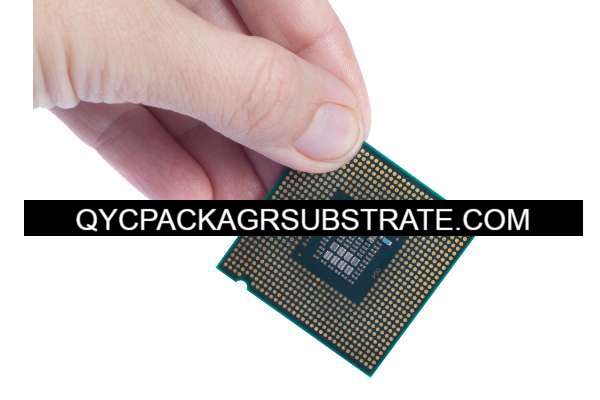
In the dynamic realm of electronic packaging, Ball Grid Array (BGA) stands out as a crucial innovation. It refers to a type of integrated circuit packaging that utilizes an array of solder balls arranged in a grid beneath the package. This distinctive design replaces traditional leads, offering improved electrical performance, reduced inductance, and enhanced thermal characteristics.
The structure of a BGA package is characterized by its compact size and the presence of a substrate, which serves as the foundation for the integrated circuit components. The solder balls, strategically arranged in a grid pattern, establish the electrical connections between the integrated circuit and the circuit board. This design not only maximizes the use of available space but also facilitates efficient heat dissipation.
Key Components of a BGA Package
To comprehend the intricacies of BGA packages, it is essential to delve into their key components. These include the integrated circuit or chip, the substrate, solder balls, and often a heat spreader. The substrate, in particular, plays a pivotal role in providing mechanical support and electrical connectivity.
The chip, housing the actual electronic components, is mounted on the substrate. Solder balls, typically made of lead-free alloys, connect the chip to the underlying circuit board, ensuring a secure and reliable electrical interface. Additionally, some BGA packages incorporate a heat spreader to enhance thermal management, dissipating heat generated during operation.
Evolution of BGA Technology in the Electronics Industry
The evolution of BGA technology has been instrumental in reshaping the landscape of electronic packaging. Traditionally, devices employed through-hole and surface-mount packages, each with its own set of limitations. BGA emerged as a revolutionary solution, offering advancements in miniaturization, electrical performance, and thermal efficiency.
Over the years, BGA technology has witnessed continuous refinement, with improvements in substrate materials, manufacturing processes, and design methodologies. This evolution has been spurred by the ever-increasing demand for smaller, more powerful electronic devices across various industries. Today, BGA packages are ubiquitous in applications ranging from consumer electronics to aerospace, showcasing the adaptability and versatility of this innovative packaging solution.
The Heart of BGA: Substrate
Definition and Significance of Substrate in BGA Packages
The substrate in Ball Grid Array (BGA) packages serves as the backbone, providing structural support and electrical connectivity for the integrated circuit components. It acts as a crucial interface between the semiconductor die and the rest of the electronic system, playing a pivotal role in overall package performance.
Diverse Landscape: Types of Substrates in BGA Technology
In the realm of BGA technology, substrates come in various forms, each tailored to meet specific performance requirements. Two primary categories dominate this landscape:
Organic Substrates: Composed of polymer-based materials, organic substrates offer flexibility and cost-effectiveness. They are commonly used in consumer electronics where a balance between performance and affordability is key.
Ceramic Substrates: Known for their exceptional thermal and electrical properties, ceramic substrates are preferred in applications demanding high performance, such as aerospace and automotive electronics. Their rigidity and excellent heat dissipation capabilities make them ideal for challenging environments.
Material Properties Steering Substrate Selection
The choice of substrate material significantly influences the functionality and reliability of BGA packages. Three key material properties guide substrate selection:
Thermal Conductivity: Organic substrates typically have lower thermal conductivity compared to ceramics. The ability of a substrate to efficiently dissipate heat impacts the overall thermal performance of the BGA package, crucial for preventing overheating in high-power applications.
Dielectric Constant: The dielectric constant of a substrate material affects signal propagation and integrity. Achieving the right balance between electrical insulation and signal transmission is crucial for maintaining performance and minimizing signal loss.
CTE (Coefficient of Thermal Expansion): Matching the CTE of the substrate with that of the semiconductor die is essential to prevent stress-induced failures during temperature fluctuations. A well-matched CTE ensures structural integrity and reliability over the operational lifespan of the electronic device.
Crafting Success: Importance of Substrate Layout and Design
The layout and design of the substrate play a vital role in optimizing electrical performance and reliability. Properly designed traces, vias, and connections contribute to signal integrity, reducing the risk of signal distortion or loss. Furthermore, an efficient layout aids in thermal management, distributing heat evenly across the substrate and preventing localized hotspots that could compromise the BGA package’s performance.
In conclusion, understanding the nuanced role of the substrate in BGA packages involves considering various factors such as material choice, thermal properties, and design intricacies. This holistic approach ensures the seamless integration of BGA technology into diverse electronic applications, meeting the demands of both consumer and high-performance markets.
Unraveling the Die Package Substrate
Significance of Die Package Substrate in BGA Technology
In the intricate world of Ball Grid Array (BGA) technology, the die package substrate stands as a linchpin, playing a pivotal role in the functionality and reliability of electronic devices. This foundational component acts as the platform connecting the semiconductor die to the rest of the package, facilitating efficient electrical connections and enabling seamless communication between the integrated circuits.
The die package substrate serves as more than just a physical support for the semiconductor die; it is the critical interface that ensures the efficient transfer of signals, power, and heat. Its design and material properties directly impact the overall performance and durability of electronic devices utilizing BGA packages.
Role of Die Attach Materials
Delving deeper into the intricacies, the role of die attach materials within the die package substrate is paramount. These materials serve the crucial function of bonding the semiconductor die to the substrate, establishing a reliable electrical connection. The choice of die attach materials significantly influences thermal conductivity, mechanical strength, and overall electrical performance.
Modern BGA packages demand die attach materials that not only provide a secure bond but also enhance thermal dissipation, ensuring optimal functioning even under demanding conditions. Engineers carefully select and optimize these materials to strike a delicate balance between electrical conductivity and effective heat transfer, ultimately contributing to the longevity and efficiency of the electronic device.
Thermal Considerations in Die Package Substrates
Thermal considerations are of utmost importance in the realm of die package substrates, addressing the challenges posed by the continuous miniaturization and increased power density of electronic components. Efficient thermal management is essential to prevent overheating and ensure the reliability of the semiconductor die.
Die package substrates must exhibit high thermal conductivity and a low coefficient of thermal expansion (CTE) to effectively dissipate heat generated during operation. Engineers meticulously design substrates with thermal vias and optimized layouts to enhance heat dissipation, maintaining the temperature within permissible limits. These considerations are critical for preventing performance degradation and ensuring the longevity of electronic devices.
Advances in Die Package Substrate Technology
The landscape of die package substrate technology is witnessing continuous evolution, driven by the demand for enhanced performance and miniaturization. Recent advancements encompass a spectrum of innovations, ranging from novel materials to sophisticated manufacturing processes.
Nanotechnology has introduced materials with improved thermal conductivity and mechanical properties, pushing the boundaries of what die package substrates can achieve. Additionally, innovative manufacturing techniques, such as 3D printing and advanced laser processing, have enabled the creation of intricately designed substrates that optimize signal integrity and thermal performance.
As technology marches forward, the die package substrate remains a focal point of research and development, with engineers striving to push the boundaries of what is possible in the realm of BGA technology. These continuous advancements pave the way for more compact, efficient, and robust electronic devices, underlining the integral role of die package substrates in shaping the future of electronic engineering.
Challenges and Solutions
Common Challenges Associated with BGA Substrate Technology
Thermal Management Challenges
Keyword Integration: Maintaining optimal temperatures within the BGA package.
Discussion: Thermal issues, such as hotspots, pose a common challenge in BGA substrate technology, affecting the performance and reliability of electronic devices.
Electromagnetic Interference (EMI)
Keyword Integration: Reducing EMI for enhanced signal integrity.
Discussion: EMI interference can compromise the functionality of electronic components, necessitating strategic substrate design to mitigate these challenges.
Material Compatibility
Keyword Integration: Ensuring compatibility between substrate materials and electronic components.
Discussion: Mismatched material properties can lead to reliability issues, emphasizing the need for careful selection and compatibility testing.
Innovative Solutions and Advancements in Substrate Design
Advanced Material Technologies
Keyword Integration: Leveraging cutting-edge materials for improved substrate performance.
Discussion: Integration of materials with enhanced thermal conductivity and reduced CTE addresses challenges and contributes to overall BGA package reliability.
3D Packaging Techniques
Keyword Integration: Implementing 3D packaging for optimized space utilization.
Discussion: Innovations in substrate design, including 3D stacking, enable compact and efficient layouts, overcoming spatial limitations and enhancing overall performance.
Embedded Cooling Solutions
Keyword Integration: Incorporating embedded cooling mechanisms for efficient thermal management.
Discussion: Innovative cooling solutions, such as embedded heat sinks and thermal vias, contribute to overcoming thermal challenges and ensuring sustained performance.
Impact of Substrate Choices on Overall BGA Package Performance
Reliability and Longevity
Keyword Integration: Influence of substrate choices on the long-term reliability of BGA packages.
Discussion: Optimal substrate selection directly impacts the lifespan of electronic devices, emphasizing the importance of considering long-term reliability in design decisions.
Signal Integrity and Speed
Keyword Integration: Impact of substrate characteristics on signal integrity and data transmission speed.
Discussion: Substrate choices play a critical role in maintaining signal integrity and supporting high-speed data transmission, directly influencing overall BGA package performance.
Cost Considerations
Keyword Integration: Balancing performance requirements with cost-effective substrate choices.
Discussion: The economic aspect of substrate selection is crucial, and finding a balance between performance and cost is essential for widespread adoption of BGA packages in various applications.
This section explores the challenges faced in BGA substrate technology, introduces innovative solutions, and underscores the far-reaching impact of substrate choices on the overall performance and reliability of electronic devices.