
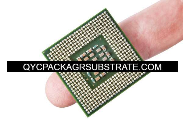
Advanced packaging substrate manufacturer. we can produce the best samllest bump pitch with 100um, the best smallest trace are 9um. and the smallest gap are 9um. most of the design are 15um to 30um trace and spacing.
In the realm of cutting-edge electronic devices, Advanced Packaging Substrate (APS) emerges as a linchpin, wielding substantial influence. It takes the form of a crucial material or framework that provides support and interconnectivity to the sundry electronic components dwelling within semiconductor devices. Serving as a nexus, the substrate expedites the exchange of information and the judicious distribution of power across the diverse precincts of the device.
Distinguished attributes and functions characterizing Advanced Packaging Substrates encompass:
Connectivity Nexus: APS furnishes a substratum for the amalgamation of integrated circuits, laying the groundwork for an intricate lattice of electrical conduits. This seamless architecture facilitates the fluid transmission of data and signals between the disparate components nestled within the semiconductor device.
Signal Prowess: The substrate is meticulously crafted to navigate signals with finesse, ensuring an adept communication milieu within the confines of the device.
Power Propagation: APS streamlines the internal propagation of power, ensuring that each constituent receives the requisite electrical impetus for optimal operational prowess.
Thermal Governance: Given the escalating intricacy and diminution of electronic devices, APS often integrates features designed for the adroit management and dissipation of thermal energy, thereby bolstering the device’s overall resilience and efficiency.
Scale-down Synthesis: APS technologies usher in a paradigm where electronic components undergo scale-down synthesis, ushering in a new era of pint-sized and consolidated devices. This transformative trend is particularly pivotal in sectors where spatial constraints reign supreme, such as in the realms of mobile devices and wearable technology.
Augmented Performance: The intrinsic design and composition of APS wield the potential to substantially augment electrical performance, mitigating signal losses, and elevating the overall functional acumen of the semiconductor device.
Embodiments of Advanced Packaging Substrate technologies encompass a diverse spectrum, with exemplars like System-in-Package (SiP), 2.5D packaging, and 3D packaging, each showcasing nuanced levels of integration and efficacy. As technological strides persist, the voracious appetite for more intricate packaging solutions propels the continual evolution of inventive substrate materials and designs, attuned to the ever-evolving exigencies of electronic devices.
What Specific Functions Does Advanced Packaging Substrate Have?
In the intricate world of electronic devices, Advanced Packaging Substrate (APS) emerges as a versatile player, seamlessly performing a myriad of pivotal functions. Here’s a closer look at its roles:
Nerve Center of Connectivity: APS takes center stage as the pivotal hub for connecting integrated circuits and diverse electronic components. It sets the stage for a fluid exchange of data and signals, fostering connectivity between different facets of the device.
Signal Choreographer: With meticulous design, the substrate becomes a skilled choreographer of signals, ensuring a harmonious and efficient communication network within the device. It crafts pathways that allow electrical signals to gracefully traverse between integrated circuits.
Power Maestro: APS assumes the role of a maestro in distributing electrical power within the device. Its precise orchestration ensures each component receives the exact power needed for optimal performance, enhancing the overall symphony of the electronic device.
Thermal Virtuoso: In the face of escalating miniaturization challenges, APS showcases its prowess in thermal management. It deftly dissipates the heat generated during operation, preventing overheating and preserving the reliability of the device.
Size Alchemist: APS, through its transformative technologies, plays the role of an alchemist, contributing to the downsizing of electronic components. This transformative process gives rise to smaller and more compact devices, particularly crucial in the domains of mobile devices and wearables.
Electrical Performance Virtuoso: The design and materials chosen for APS are geared towards elevating the electrical performance of the device. This includes minimizing signal losses, taming electromagnetic interference, and orchestrating an overall symphony of enhanced functionality in the semiconductor device.
Architect of 3D Integration: APS stands as the architect in the realm of 3D packaging technologies, enabling the artful stacking of multiple layers of integrated circuits. This vertical integration not only enhances the performance but also crafts an efficient spatial composition.
Guardian of Durability: Beyond its technical roles, APS assumes the role of a guardian, providing a protective shield for integrated circuits against environmental elements. This safeguarding significantly contributes to the overall durability and endurance of the electronic device.
In essence, Advanced Packaging Substrate emerges not just as a functional component but as a versatile artist, adeptly conducting the symphony of connectivity, power distribution, thermal regulation, and enhanced performance in the dynamic landscape of modern electronic devices.
What Are the Different Types of Advanced Packaging Substrate?
The realm of Advanced Packaging Substrates (APS) unfolds with a tapestry of diverse technologies, each tailored to meet the ever-shifting demands of electronic devices. Let’s delve into the intricacies of various APS types:
System-in-Package (SiP): SiP takes the spotlight by seamlessly integrating multiple functional components, including chips and interconnects, into a unified package. This holistic approach champions compactness and efficiency, ushering in an amplified overall performance.
2.5D Packaging: Engaging in the dance of 2.5D packaging involves artfully stacking multiple dies on an interposer—a dedicated substrate fostering connectivity between layers. This choreography amplifies integration capabilities and orchestrates a performance boost.
3D Packaging: In the symphony of 3D packaging, semiconductor dies ascend vertically, conducting a harmonious composition that unfolds advantages like enhanced performance, a minimized footprint, and a more efficient dissipation of heat.
Fan-Out Wafer-Level Packaging (FO-WLP): FO-WLP takes center stage with its dynamic redistribution of chip connections across a larger canvas, enabling an ensemble of components and superior thermal performance. This act finds resonance, especially in the realm of mobile devices.
Embedded Substrate: The embedded substrate takes on the role of an invisible hand, seamlessly integrating into the device itself. This discreet integration crafts a compact solution, a silent yet powerful player in applications with strict spatial constraints.
Flip-Chip Packaging: The flip-chip packaging dance unfolds with the semiconductor die taking a bow, facing downward, directly connecting with the substrate. This poised configuration shortens interconnections, resulting in a performance crescendo.
Ceramic Substrate: A virtuoso in thermal conductivity, the ceramic substrate takes the stage where efficient heat dissipation is paramount—think high-performance computing and power electronics.
Organic Substrate: Crafted from materials like FR-4, the organic substrate plays a versatile role in standard printed circuit boards (PCBs) and various packaging solutions. It’s a cost-effective ensemble widely embraced in the symphony of consumer electronics.
Glass Interposer: The glass interposer steps into the limelight, providing a platform for the stacked semiconductor dies. With a unique blend of electrical performance, thermal properties, and scalability, it crafts an avant-garde performance.
Interposer-based Packaging: In the ballet of interposer-based packaging, an additional layer gracefully interposes itself between semiconductor dies, facilitating intricate connectivity. This delicate dance supports finer pitch connections and serves a multitude of functions.
This cavalcade of APS types unfolds a myriad of choices for designers, allowing them to compose a symphony of performance, size, and functionality tailored to the specific nuances of each application. The selection of the right substrate type emerges as a nuanced art, considering the unique characteristics of each performance—nature, demands, and budget.
How is Advanced Packaging Substrate Related to IC Packaging?
Advanced Packaging Substrate (APS) and IC (Integrated Circuit) packaging share an intimate relationship, working in tandem to shape the form and functionality of electronic devices. Let’s explore the connections between these two crucial elements:
Central Integration Hub: APS serves as the central hub for integrating various components within an IC package. It’s the canvas upon which the integrated circuit die, alongside other elements like interconnects and passive components, comes together to form a cohesive unit.
Electrical Networking: Both IC packaging and APS are architects of electrical connectivity. APS functions as the conduit through which electrical signals traverse, fostering seamless communication between different elements within the packaged IC.
Guiding Signal Pathways: Signal routing is a shared responsibility of IC packaging and APS. The intricate pathways carved out in the substrate guide electrical signals between the integrated circuit and other components, ensuring a harmonious flow of data.
Power Dissemination: Within the realm of IC packaging, APS takes charge of power distribution. It orchestrates the delivery of electrical power to diverse components, guaranteeing that each part of the integrated circuit receives the requisite power for optimal performance.
Heat Harmonization: Thermal management is a shared concern for both APS and IC packaging. Effectively dissipating heat is crucial to prevent overheating and uphold the reliability and efficiency of the integrated circuit in its packaged form.
Size Refinement and Optimization: APS technologies contribute to the overarching goal of size reduction, aligning with the aspirations of IC packaging. Smaller, more compact packages are sought after, especially in applications where spatial constraints are a defining consideration.
Exploration of Advanced Techniques: IC packaging explores various advanced packaging techniques, such as System-in-Package (SiP), 2.5D packaging, and 3D packaging. APS serves as the canvas for implementing these techniques, enabling higher integration levels and pushing the boundaries of performance and functionality.
In essence, Advanced Packaging Substrate emerges as the foundational canvas for the intricate artistry of IC packaging. Together, they sculpt the landscape of modern electronic devices, dictating their size, efficiency, and performance capabilities. The synergy between APS and IC packaging is a dynamic collaboration at the heart of technological innovation.
How Does Advanced Packaging Substrate Differ from Traditional PCBs?
In the intricate tapestry of electronic components, Advanced Packaging Substrate (APS) and traditional Printed Circuit Boards (PCBs) don distinct roles, weaving their narratives with unique designs, functions, and applications. Let’s delve into the nuances that set them apart:
Integration Choreography:
Advanced Packaging Substrate (APS): APS takes the lead in orchestrating an intricate three-dimensional integration ballet. Its expertise lies in stacking layers and components, achieving a level of complexity and integration that transcends the capabilities of traditional PCBs.
Traditional PCBs: Traditional PCBs perform on a two-dimensional stage, perfectly suited for less complex electronic circuits. They find their rhythm in applications where intricate integration is not the primary focus.
Component Fusion:
APS: APS is tailored for the fusion of diverse components, harmonizing semiconductor dies, passive elements, and interconnects. It often employs sophisticated packaging technologies like System-in-Package (SiP) or 3D packaging.
Traditional PCBs: In the realm of traditional PCBs, integration involves fundamental electronic components like resistors and transistors on a flat surface, without reaching the complexity levels of APS.
Downsizing Elegance:
APS: APS technologies contribute to the art of downsizing, crafting devices with a smaller and more compact footprint.
Traditional PCBs: While traditional PCBs can adopt reduced dimensions, they generally trend toward larger sizes when compared to the intricately packed configurations achievable with APS.
Signal Composition Complexity:
APS: APS engages in the composition of intricate signal pathways, choreographing communication among densely packed components.
Traditional PCBs: Signal routing on traditional PCBs tends to be less complex, with straightforward traces connecting components in a two-dimensional arrangement.
Application Symphony:
APS: APS takes center stage in advanced electronic devices such as smartphones and wearables, as well as in high-performance computing, where space optimization and intricate integration are paramount.
Traditional PCBs: Traditional PCBs find their roles across a diverse spectrum of electronic devices, from everyday consumer electronics to industrial equipment, catering to applications with less demanding integration requirements.
Material Melody:
APS: APS gracefully dances with specialized materials like organic substrates, ceramics, or glass, tailored to meet the demands of advanced packaging technologies.
Traditional PCBs: Traditional PCBs, grounded in practicality, often embrace cost-effective materials like FR-4, well-suited for applications where stringent integration and miniaturization are not critical.
In essence, Advanced Packaging Substrate and traditional PCBs each take the stage with their unique performances, catering to electronic systems at different complexity levels. APS excels in the finesse of advanced packaging, enabling higher integration and miniaturization, while traditional PCBs find their rhythm in applications with less complex electronic circuits.
What is the Main Structure and Production Technology of Advanced Packaging Substrate?
The structural composition and production technology of Advanced Packaging Substrate (APS) represent a dynamic interplay of materials and processes tailored to meet the intricate demands of modern electronic devices. Let’s delve into the architectural tapestry and manufacturing intricacies:
Architectural Ensemble of Advanced Packaging Substrate:
Foundation Material:
APS takes its form on a foundational material, which can be organic, ceramic, or glass. The choice hinges on specific requirements such as thermal conductivity, electrical characteristics, and cost considerations.
Conductive Circuitry Layers:
Multiple layers of conductive circuitry grace the substrate, weaving a network of traces and interconnects to facilitate the seamless flow of electrical signals.
Insulating Dielectric Layers:
Intervening dielectric layers gracefully separate conductive traces, preventing interference and ensuring insulation to maintain proper electrical isolation.
Through-Silicon Vias (TSVs):
In the realm of advanced packaging, especially in the 3D configuration, Through-Silicon Vias (TSVs) may take center stage. These vertical interconnects traverse the substrate, connecting different layers or stacked dies.
Bump and Pad Ballet:
Bump and pad structures elegantly adorn the substrate, forming the critical links between the substrate and semiconductor dies. This choreography facilitates the transmission of signals, power, and data.
Integration of Passive Components:
Some APS designs showcase the integration of passive components directly onto the substrate, including resistors and capacitors. This elevates overall integration density and performance.
Symphony of Production Technology:
Photolithographic Artistry:
Photolithography assumes a pivotal role, defining intricate circuit patterns on the substrate. It employs light to transfer the design onto the substrate through a photoresist layer.
Deposition Elegance:
Thin films of conductive and dielectric materials gracefully descend onto the substrate through deposition techniques like chemical vapor deposition (CVD) or physical vapor deposition (PVD).
Etching Choreography:
Etching, a masterful performance, delicately removes excess material and sculpts the defined circuit patterns. Whether through wet or dry etching, the result is precision and refinement.
Plating Brilliance:
The plating act takes the stage, electroplating to build up metal layers for bumps and pads. This enhances the conductivity, ensuring the brilliance of critical connection points.
Bumping Artistry:
Bumping unfolds as solder or conductive materials are artistically added to create connections between the substrate and semiconductor dies.
Assembly and Packaging Symphony:
The grand finale involves assembly processes where semiconductor dies and other components join the APS. Techniques such as flip-chip bonding or wire bonding contribute to the harmonious packaging.
Testing and Inspection Crescendo:
Rigorous testing and inspection crescendo into the production flow, ensuring the APS’s integrity and functionality. Electrical tests and meticulous visual inspections contribute to the symphony of quality assurance.
3D Integration Overture (Optional):
In certain acts where 3D packaging takes the spotlight, additional processes such as Through-Silicon Via (TSV) fabrication and die stacking elegantly weave into the production narrative.
The production technology for APS is akin to a constantly evolving masterpiece, incorporating new materials and technologies to resonate with the ever-evolving demands of contemporary electronic devices.
FAQs
How Does APS Deviate from Traditional PCBs?
APS and traditional Printed Circuit Boards (PCBs) diverge in terms of integration intricacy, miniaturization capabilities, and adaptability to advanced packaging technologies. APS, with its penchant for intricate integration and potential for 3D configurations, stands in contrast to traditional PCBs, which are two-dimensional and more suited for less complex electronic circuits.
What Encompasses the Production Technology in APS Manufacturing?
The symphony of production technologies in APS manufacturing includes the artistry of photolithography for delineating circuit patterns, the deposition of thin films using techniques like Chemical Vapor Deposition (CVD) or Physical Vapor Deposition (PVD), the choreography of etching to carve precise circuit patterns, the brilliance of plating to enhance conductivity, the artistry of bumping for establishing connections, and the grand finale of assembly processes such as flip-chip bonding or wire bonding. The crescendo of rigorous testing and inspection ensures the harmonious quality of the final composition.
What Role Does APS Play in Thermal Management?
APS assumes a pivotal role in thermal management by influencing the dissipation of heat emanating from electronic components. Whether through the selection of materials with enhanced thermal conductivity or specific substrate configurations, APS ensures the reliability and efficiency of integrated circuits by effectively managing thermal concerns.
Is APS Governed by Standardization?
While certain aspects of APS adhere to industry standards, the technology itself is a tapestry of diversity and continuous evolution. The dynamic nature of APS allows for variations in design and production, making it a fluid field with diverse approaches and innovative solutions.
How Does APS Facilitate 3D Integration?
APS serves as the facilitator for 3D integration by providing a canvas for the vertical stacking of semiconductor dies. Through technologies like Through-Silicon Vias (TSVs), connections are established between different layers, ushering in a three-dimensional configuration that elevates performance and density.
What Challenges Mark the Landscape of APS Development?
The journey of APS development is marked by challenges that include achieving higher integration without compromising reliability, navigating thermal intricacies in densely packed configurations, and adapting to the nuances of emerging technologies. Ongoing efforts in standardization and material innovations form the tapestry of solutions aimed at overcoming these challenges and propelling the advancement of APS technology.
Conclusion
In conclusion, Advanced Packaging Substrate (APS) emerges as a linchpin in the intricate world of electronic components, contributing significantly to the evolution of modern devices. As a structural and electrical foundation, APS plays a pivotal role in facilitating the integration of semiconductor dies, passive components, and interconnects. The diverse landscape of APS includes various types, from System-in-Package (SiP) to 3D packaging, each tailored to meet specific demands in terms of integration, performance, and application contexts.
APS stands apart from traditional Printed Circuit Boards (PCBs) through its ability to navigate intricate integration, employ advanced packaging technologies, and contribute to the ongoing trend of miniaturization. The production technology involved in APS manufacturing resembles a symphony, involving precise processes such as photolithography, deposition, etching, plating, and assembly techniques. Rigorous testing and inspection form the crescendo, ensuring the quality and reliability of the final product.
The versatility of APS extends across a diverse spectrum of electronic devices, from ubiquitous smartphones to high-performance computing systems. Its role in miniaturization is particularly noteworthy, achieved through techniques like 2.5D and 3D packaging that enable the vertical stacking of semiconductor dies.
Thermal management is another critical facet of APS, influencing the dissipation of heat from electronic components. Whether through material selection or specific substrate configurations, APS contributes to the reliability and efficiency of integrated circuits.
While APS adheres to certain industry standards, its dynamic nature allows for flexibility in design and production, reflecting a field that continually adapts to emerging technologies and requirements. Challenges in APS development, such as achieving higher integration and addressing thermal concerns, are met with ongoing efforts in standardization and material innovations.
In essence, Advanced Packaging Substrate encapsulates the essence of innovation and adaptability in the ever-evolving landscape of electronic systems. Its presence is not only foundational but transformative, shaping the future of electronic devices with each advancement in integration, miniaturization, and performance.