
Ajinomoto(ABF) Filp Chip Substrate Manufacturer
Ajinomoto(ABF) Filp Chip Substrate Manufacturer,Ajinomoto (ABF) Flip Chip Substrates are high-performance circuit boards designed for advanced flip chip packaging. ABF, or Ajinomoto Build-up Film, is a type of resin used in these substrates to provide excellent dielectric properties and mechanical strength. These substrates feature a multi-layer build-up structure that supports fine-pitch flip chip interconnections, enabling high-density and high-speed data processing. The ABF material enhances thermal and electrical performance, making these substrates ideal for applications in high-end computing, telecommunications, and consumer electronics. Ajinomoto flip chip substrates are renowned for their reliability and efficiency, contributing to the compact and high-functioning designs of modern electronic devices.
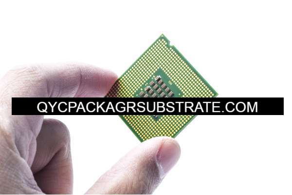
What is Ajinomoto (ABF) Flip Chip Substrate?
Ajinomoto Build-up Film (ABF) Flip Chip Substrate is a crucial electronic material widely used in modern semiconductor packaging technology. Developed by Ajinomoto, this high-performance substrate serves as an intermediary between semiconductor chips and printed circuit boards (PCBs). The unique aspects of ABF substrates include their excellent electrical performance, mechanical strength, and thermal stability, making them the ideal choice for high-density interconnects and high-performance electronic devices.
ABF Flip Chip Substrate is primarily used in Flip Chip packaging technology. This technique involves directly soldering the chip onto the substrate by flipping the chip, thereby achieving higher interconnect density and shorter signal transmission paths. This not only enhances chip performance but also reduces the size and weight of the package, making it highly suitable for high-performance and miniaturized electronic products like smartphones, tablets, and high-performance computing devices.
A significant feature of Ajinomoto ABF is its excellent coefficient of thermal expansion (CTE) matching performance. This ensures good compatibility with silicon chips and PCBs during temperature changes, preventing stress and damage caused by thermal expansion mismatches. Additionally, ABF has excellent electrical insulation properties and low-loss characteristics, ensuring the quality of high-speed signal transmission.
Furthermore, Ajinomoto continually improves and optimizes ABF materials to meet the increasingly complex demands of semiconductor packaging. The new generation of ABF materials has shown significant improvements in thickness, strength, and processing performance, further promoting the trend of performance enhancement and miniaturization of electronic products.
In summary, Ajinomoto ABF Flip Chip Substrate plays a vital role in modern electronic packaging. Its superior performance and continuous innovation drive the development of electronic technology, making smaller, faster, and more efficient electronic devices possible.
Ajinomoto(ABF) Filp Chip Substrate Manufacturer
What are the Design Guidelines for Ajinomoto (ABF) Flip Chip Substrate?
Design guidelines for Ajinomoto Build-up Film (ABF) Flip Chip Substrate are crucial for ensuring optimal performance and reliability in electronic devices. These guidelines help designers and engineers maximize the benefits of ABF substrates in flip chip packaging. Here are some key considerations:
- Thermal Management: Ensure effective thermal management to accommodate the heat generated by high-performance chips. Adequate heat dissipation and thermal vias are essential to maintain the reliability of the flip chip assembly.
- Pad Design:Design the solder pads on the substrate to match the chip’s bump pitch and size accurately. The pad layout should ensure proper alignment and contact with the chip bumps, minimizing the risk of soldering defects.
- Electrical Performance: Optimize the trace and via design to minimize signal loss and interference. Use appropriate trace widths and via sizes to handle the high-frequency signals and reduce impedance mismatches.
- Coefficient of Thermal Expansion (CTE) Matching: Pay attention to the CTE matching between the ABF substrate, silicon chip, and PCB. Proper CTE matching helps prevent mechanical stress and potential damage due to thermal cycling.
- Mechanical Strength: Ensure that the substrate has adequate mechanical strength to withstand the stresses during manufacturing and operation. Consider the substrate’s rigidity and impact resistance to maintain structural integrity.
- Design for Manufacturability:Design the substrate with manufacturing constraints in mind, such as minimum trace widths, spacing requirements, and layer stack-ups. Ensure that the design can be efficiently produced and assembled.
- Signal Integrity: Implement design practices to enhance signal integrity, such as controlled impedance traces and proper grounding techniques. Use simulation tools to analyze and optimize the signal paths.
- Testability: Incorporate test points and design features that facilitate electrical testing and inspection of the flip chip assembly. This helps in early detection of potential issues and ensures the quality of the final product.
- Reliability Testing: Subject the design to reliability testing, including thermal cycling, thermal shock, and mechanical stress tests. Validate the substrate’s performance under various environmental conditions to ensure long-term reliability.
- Compliance with Standards: Adhere to industry standards and guidelines for flip chip packaging, such as IPC standards and JEDEC specifications. Compliance with these standards ensures compatibility and reliability across different applications.
By following these design guidelines, engineers can effectively leverage the advantages of Ajinomoto ABF Flip Chip Substrates, ensuring high performance, reliability, and manufacturability in advanced electronic devices.
What is the Fabrication Process for Ajinomoto (ABF) Flip Chip Substrate?
The fabrication process for Ajinomoto Build-up Film (ABF) Flip Chip Substrate involves several critical steps to create high-performance and reliable substrates for advanced semiconductor packaging. Here’s an overview of the process:
- Substrate Preparation: Start with a base material, typically a thin copper foil or a pre-laminated core. This forms the foundation for the ABF build-up layers. The base material is cleaned and treated to ensure proper adhesion of subsequent layers.
- Build-Up Layer Application: Apply a build-up film (ABF) to the base material. This film is a polymer resin with high performance in terms of electrical and thermal properties. The ABF film is laminated onto the base material using heat and pressure.
- Photoimaging and Etching: Once the build-up layer is applied, it is subjected to photolithography. A photoresist layer is coated on top, and the desired circuit patterns are exposed using ultraviolet (UV) light. The exposed areas are developed and then etched away to form the necessary circuit patterns and vias.
- Via Formation: For multi-layer substrates, vertical interconnections (vias) are created to connect different layers of the substrate. This involves drilling or laser ablation to form vias, followed by plating with copper to establish electrical connections between layers.
- Layer-by-Layer Build-Up: Additional layers of ABF film are sequentially added, and the photoimaging and etching processes are repeated. Each layer is carefully aligned and bonded to the previous layer to build up the substrate to the required thickness and complexity.
- Pad Formation and Plating: Solder pads and other interconnect features are formed on the surface of the substrate. This is done by depositing and patterning copper on the substrate, followed by electroplating to enhance pad thickness and improve solderability.
- Chemical Mechanical Planarization (CMP): The surface of the substrate is polished to achieve a smooth and even finish. CMP removes any excess material and ensures that the surface is flat and ready for further processing.
- Final Inspection and Testing: The substrate undergoes rigorous inspection and testing to ensure it meets quality standards. This includes checking for defects, verifying electrical performance, and ensuring dimensional accuracy.
- Dicing and Packaging: Once the substrate has passed inspection, it is diced into individual units if required. The final substrates are then packaged for shipment or further assembly into electronic devices.
- Reflow and Assembly: If the substrate is being used for flip chip packaging, the chip is aligned and attached to the substrate using solder bumps. The assembly is then subjected to a reflow process to melt the solder and form strong electrical connections between the chip and the substrate.
This fabrication process ensures that Ajinomoto ABF Flip Chip Substrates meet the high standards required for advanced semiconductor applications, providing excellent electrical performance, thermal management, and reliability.
How Do You Manufacture Ajinomoto (ABF) Flip Chip Substrate?
Manufacturing Ajinomoto Build-up Film (ABF) Flip Chip Substrate involves a detailed and precise process to ensure high performance and reliability. Here’s a step-by-step overview of how to manufacture these substrates:
- Material Selection: Begin with selecting high-quality Ajinomoto ABF material, known for its excellent electrical and thermal properties. The material is typically in the form of a resin film that will be built up in layers.
- Base Substrate Preparation: Start with a base substrate, usually a thin copper-clad laminate. This base will support the build-up layers and form the initial layer of the substrate. The base material is cleaned and treated to enhance adhesion with the ABF film.
- Lamination of ABF Film:Apply the ABF film to the base substrate using a lamination process. The film is positioned on the substrate and then subjected to heat and pressure to bond the film firmly to the base material.
- Photoresist Coating and Patterning: A photoresist layer is applied over the ABF film. This layer will be patterned to create the circuit design. The photoresist is exposed to UV light through a mask that defines the desired circuit patterns. The exposed photoresist is then developed to reveal the pattern.
- Etching: After patterning, the substrate is subjected to an etching process to remove the unprotected ABF material. This creates the circuit traces and via openings according to the design.
- Via Formation: For multi-layer designs, vias are formed to create electrical connections between different layers. This involves drilling or laser ablation to form via holes, followed by plating with copper to establish electrical continuity.
- Build-Up Layer Addition: Additional layers of ABF film are applied and processed similarly to the initial layer. This build-up process is repeated as necessary to achieve the required number of layers and circuit complexity.
- Pad Formation and Plating: Solder pads and other interconnect features are formed by depositing and patterning copper on the surface of the substrate. Electroplating is used to enhance the thickness and solderability of these pads.
- Chemical Mechanical Planarization (CMP): The substrate’s surface is polished using CMP to ensure a smooth and flat surface. This step removes excess material and ensures that the surface is suitable for the final assembly.
- Inspection and Testing: Conduct thorough inspection and testing of the substrate to ensure it meets quality standards. This includes checking for defects, verifying circuit integrity, and ensuring the substrate meets dimensional and performance specifications.
- Dicing and Packaging:After passing inspection, the substrate is diced into individual units if required. The final products are packaged for shipment or further assembly into electronic devices.
- Flip Chip Assembly: For substrates used in flip chip packaging, align and attach the semiconductor chip to the substrate using solder bumps. Perform a reflow process to melt the solder and establish electrical connections between the chip and the substrate.
By following these steps, manufacturers can produce high-quality Ajinomoto ABF Flip Chip Substrates that offer superior performance in advanced electronic applications, supporting high-speed, high-density, and reliable connections.
How Much Should Ajinomoto (ABF) Flip Chip Substrate Cost?
The cost of Ajinomoto Build-up Film (ABF) Flip Chip Substrate can vary widely depending on several factors, including design complexity, layer count, substrate size, and order volume. Here’s a detailed overview of the factors influencing the cost:
- Design Complexity: More complex designs with higher density interconnects, finer pitch, and multiple layers will generally be more expensive. Advanced designs require more precise manufacturing processes and quality control, increasing the overall cost.
- Layer Count: The number of build-up layers in the substrate affects the cost. Each additional layer requires more material, processing time, and quality checks, leading to higher costs for multi-layer substrates.
- Substrate Size: Larger substrates or substrates with custom dimensions will incur higher costs due to increased material usage and processing time. Custom sizes and shapes often involve additional setup and tooling costs.
- Volume of Order: The quantity of substrates ordered plays a significant role in determining the cost. Higher volumes typically benefit from economies of scale, reducing the cost per unit. Conversely, smaller orders may have higher per-unit costs due to lower production volumes.
- Material Specifications: The specific type and grade of ABF material used, as well as any special requirements for thermal or electrical performance, can influence the cost. Premium materials with enhanced properties may be more expensive.
- Manufacturing Process: The complexity and precision of the manufacturing process impact the cost. Processes involving advanced photolithography, multiple build-up layers, and high-precision etching and plating contribute to higher costs.
- Testing and Quality Control:Comprehensive testing and quality control measures to ensure substrate reliability and performance add to the cost. High standards of inspection and testing are crucial for high-performance applications but can increase the overall price.
- Custom Features: Any additional features, such as custom pad designs, unique via arrangements, or special surface treatments, can also affect the cost. Customizations require additional design and manufacturing effort.
As a rough estimate, the cost of ABF Flip Chip Substrates can range from a few dollars to several hundred dollars per unit, depending on the factors mentioned above. For specific pricing, it is best to consult with manufacturers or suppliers who can provide quotes based on detailed requirements and order specifications.
In summary, the cost of Ajinomoto ABF Flip Chip Substrates is influenced by design complexity, layer count, substrate size, order volume, material specifications, manufacturing processes, testing requirements, and any custom features. Understanding these factors can help in estimating costs and making informed decisions for procurement.
What is the Base Material for Ajinomoto (ABF) Flip Chip Substrate?
The base material for Ajinomoto Build-up Film (ABF) Flip Chip Substrate is a critical component in the substrate’s overall structure, providing the foundation upon which the build-up layers are applied. Here’s a detailed overview of the base material used:
- Copper-Clad Laminate: The primary base material for ABF Flip Chip Substrates is usually a copper-clad laminate. This consists of a thin layer of copper foil bonded to a dielectric material, such as epoxy resin or other high-performance polymers. The copper layer provides the electrical interconnections, while the dielectric material offers insulation and mechanical support.
- Dielectric Layer: The dielectric material in the base laminate is chosen for its electrical insulation properties and thermal stability. Common dielectric materials include epoxy resins, polyimide, and other high-performance polymers. These materials are selected based on their ability to withstand thermal cycling and provide reliable electrical insulation.
- Glass-Fiber Reinforced Materials: In some cases, the base material may include glass fiber reinforcement to enhance mechanical strength and rigidity. This reinforcement helps maintain the substrate’s structural integrity during the manufacturing process and in final applications.
- Pre-Laminated Core: For certain designs, a pre-laminated core may be used. This core consists of multiple layers of dielectric material with embedded copper circuitry. The pre-laminated core provides a foundation for additional build-up layers and simplifies the manufacturing process for multi-layer substrates.
- Thermal and Electrical Properties: The choice of base material impacts the thermal and electrical performance of the ABF Flip Chip Substrate. High thermal conductivity and low thermal expansion coefficients are desirable to ensure effective heat dissipation and prevent warping or delamination. Electrical properties such as low dielectric loss and high insulation resistance are also important for maintaining signal integrity.
- Surface Treatment:The surface of the base material is often treated to improve adhesion with the ABF film. This may include surface roughening or coating with adhesion-promoting agents to ensure a strong bond between the base material and the build-up layers.
- Custom Materials: Depending on specific requirements, custom base materials may be used. These materials are engineered to meet particular performance criteria, such as enhanced thermal management, improved electrical characteristics, or specialized mechanical properties.
In summary, the base material for Ajinomoto ABF Flip Chip Substrates is typically a copper-clad laminate with a dielectric layer. This material provides the electrical and mechanical foundation for the substrate, supporting the build-up layers and ensuring reliable performance in high-density electronic applications. The choice of base material is crucial for achieving the desired thermal, electrical, and mechanical properties in the final substrate.
Which Company Makes Ajinomoto (ABF) Flip Chip Substrate?
Several companies currently manufacture Ajinomoto (ABF) Flip Chip Substrates, including Ajinomoto Co., Inc., IBM, Shinko Electric, Jiangsu Changjiang Electronics Technology Co., Ltd., and GlobalWafers in Taiwan. These companies have extensive experience and advanced technology in the development and production of ABF materials, providing high-performance flip chip substrates widely used in high-end electronic devices, smartphones, computers, and other high-tech products.
Ajinomoto is renowned for its high-quality ABF materials. IBM, with its leading technology in semiconductor packaging and integrated circuits, has extensive applications of ABF materials in high-performance computing and storage. Shinko Electric, based in Japan, is well-regarded for its manufacturing capabilities, and its ABF materials are widely used in electronic packaging. Changjiang Electronics Technology Co., Ltd. and GlobalWafers also have rich experience in producing and developing ABF Flip Chip Substrates, offering high-quality products and services to global customers.
Our company also has the capability to manufacture Ajinomoto (ABF) Flip Chip Substrates. Our products use high-performance ABF materials, ensuring excellent electrical performance and thermal management in high-density and high-performance applications. Our ABF Flip Chip Substrate products have the following features:
- High-Performance Materials: We use premium ABF materials to ensure stability and low loss in high-frequency and high-speed applications. Our materials offer excellent thermal stability and electrical insulation properties, meeting the demands of advanced electronic products.
- Advanced Manufacturing Process: Our company possesses advanced manufacturing equipment and technical expertise, allowing for high-precision circuit processing and lamination, ensuring high quality and reliability of our products.
- Multi-Layer Structure Design: We can design and manufacture multi-layer ABF Flip Chip Substrates according to customer specifications, catering to complex circuit applications.
- Quality After-Sales Service: We offer comprehensive after-sales service to ensure that customers receive timely technical support and solutions during usage.
- Custom Services: We provide customized ABF Flip Chip Substrate design and manufacturing services based on specific customer requirements, ensuring the products meet the exact needs of various applications.
Through continuous technological innovation and strict quality control, our ABF Flip Chip Substrate products have gained widespread recognition in the market and are extensively used in smartphones, computers, and high-performance computing fields. If you have a need for ABF Flip Chip Substrates, please feel free to contact us, and we will provide you with high-quality products and services.
In summary, whether it is material selection, manufacturing process, or after-sales service, our company is capable of producing high-quality ABF Flip Chip Substrates to meet the demands of various high-performance electronic applications.
What are the 7 Qualities of Good Customer Service?
Good customer service is essential for building strong relationships with customers and ensuring their satisfaction. Here are seven key qualities that define excellent customer service:
- Responsiveness: A good customer service team is quick to respond to customer inquiries, complaints, and requests. Timely responses demonstrate that the company values its customers and is committed to addressing their needs promptly.
- Empathy: Excellent customer service involves understanding and addressing the customer’s feelings and perspectives. Empathy helps build rapport, diffuse tense situations, and show that the company genuinely cares about the customer’s experience.
- Knowledgeability: Customer service representatives should have in-depth knowledge about the company’s products, services, and policies. This expertise enables them to provide accurate information, solve problems effectively, and guide customers through their queries.
- Patience: Patience is crucial when dealing with customers, especially in challenging situations. A patient representative listens carefully, remains calm, and works to resolve issues without rushing or becoming frustrated.
- Effective Communication:Clear and concise communication is key to good customer service. Representatives should be able to convey information in an easily understandable manner, avoiding jargon and ensuring that the customer comprehends the solution or response provided.
- Consistency: Providing consistent service across different interactions and touchpoints is important for building trust and reliability. Customers should expect the same high level of service whether they are contacting the company via phone, email, or in person.
- Problem-Solving Skills:Good customer service involves the ability to address and resolve issues effectively. Representatives should be adept at troubleshooting, finding solutions, and going the extra mile to ensure that the customer’s problem is resolved satisfactorily.
In summary, the seven qualities of good customer service are responsiveness, empathy, knowledgeability, patience, effective communication, consistency, and problem-solving skills. These qualities help create positive customer experiences, build trust, and foster long-term loyalty.
FAQs about Ajinomoto (ABF) Flip Chip Substrate
What is Ajinomoto (ABF) Flip Chip Substrate?
Ajinomoto (ABF) Flip Chip Substrate is a high-performance electronic substrate used in flip chip packaging. It is made from Ajinomoto Build-up Film (ABF), which offers excellent electrical and thermal properties, making it suitable for high-density and high-performance applications.
What are the main applications of ABF Flip Chip Substrates?
ABF Flip Chip Substrates are commonly used in high-performance computing, smartphones, tablets, and other advanced electronic devices. They are valued for their ability to support high-density interconnects and deliver reliable electrical performance.
What are the benefits of using ABF Flip Chip Substrates?
The benefits include high thermal conductivity, low electrical loss, and excellent mechanical stability. These properties enable efficient heat dissipation and reliable performance in demanding applications.
How is an ABF Flip Chip Substrate manufactured?
The manufacturing process involves layering ABF material on a base substrate, applying photoresist, patterning, etching, and adding additional build-up layers. This is followed by via formation, plating, and polishing to create the final substrate.
What are the key properties of ABF materials?
ABF materials are known for their high dielectric constant, low dielectric loss, and good thermal stability. These properties contribute to their effectiveness in high-speed and high-frequency applications.
How do ABF Flip Chip Substrates compare to other types of substrates?
ABF Flip Chip Substrates are often compared to other substrates like BT (Bismaleimide Triazine) or FR-4. ABF materials typically offer better performance in terms of signal integrity and thermal management due to their superior electrical and thermal properties.