
Aluminum nitride ceramic PCB manufacturing
Aluminum Nitride Ceramic PCB Manufacturing, Advanced production technology, various types of ceramic substrate manufacturers. Aluminum Nitride Ceramic PCBs are advanced circuit boards that utilize aluminum nitride ceramic as their substrate material. Renowned for their exceptional thermal conductivity, these PCBs efficiently dissipate heat generated by electronic components, making them ideal for high-power applications. The ceramic material also provides excellent electrical insulation, ensuring reliable performance and preventing electrical shorts. With mechanical stability and resistance to chemicals, Aluminum Nitride Ceramic PCBs offer durability and longevity in harsh operating environments. Their manufacturing involves specialized processes such as screen printing, firing, metallization, and drilling, resulting in high-quality PCBs tailored to meet stringent design specifications. These PCBs find applications in various industries, including aerospace, automotive, telecommunications, and power electronics, where thermal management and reliability are paramount. With their unique combination of properties, Aluminum Nitride Ceramic PCBs are at the forefront of technological innovation, driving advancements in electronic systems worldwide.
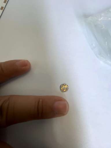
What is an Aluminum Nitride Ceramic PCB?
We are a professionalAluminum nitride ceramic PCB manufacturing, we mainly produce ultra-small bump pitch substrate, ultra-small trace and spacing packaging substrate and PCBs.
An Aluminum Nitride Ceramic PCB (Printed Circuit Board) is a type of circuit board that utilizes aluminum nitride (AlN) ceramic as its substrate material instead of traditional materials like FR4 (a type of fiberglass-reinforced epoxy).
Aluminum nitride ceramic offers several advantages over traditional PCB materials:
- Thermal conductivity: Aluminum nitride has high thermal conductivity compared to FR4, allowing for efficient dissipation of heat generated by electronic components. This property is particularly valuable in applications where thermal management is crucial, such as high-power LED lighting, power electronics, and RF/microwave devices.
- Electrical insulation: Like other ceramics, aluminum nitride is an excellent electrical insulator. This property ensures that the circuit board maintains isolation between different components and traces, preventing unwanted electrical interactions.
- Mechanical stability: Aluminum nitride has good mechanical strength and stability, making it suitable for applications where the PCB may be subjected to mechanical stress or vibrations.
- Chemical stability: Aluminum nitride is resistant to many chemicals, which enhances the reliability and durability of the PCB in harsh operating environments.
Aluminum nitride ceramic PCBs are commonly used in high-frequency and high-power applications, such as RF/microwave circuits, power amplifiers, LED modules, and automotive electronics, where their thermal and electrical properties are beneficial. However, they are typically more expensive than traditional PCB materials due to the higher cost of manufacturing and processing ceramic substrates.
What are the Aluminum Nitride Ceramic PCB Design Guidelines?
Designing PCBs with aluminum nitride ceramic substrates requires careful consideration of the material’s properties and limitations. Here are some guidelines to follow:
- Thermal Management: Aluminum nitride ceramic has excellent thermal conductivity, but effective thermal management is still crucial. Ensure proper placement of heat-generating components and consider adding thermal vias to efficiently transfer heat away from critical areas.
- Material Compatibility: Aluminum nitride ceramic has different electrical and thermal properties compared to traditional PCB materials like FR4. Ensure that the chosen components and solder materials are compatible with the ceramic substrate to prevent issues such as thermal expansion mismatch.
- Dielectric Constant: Aluminum nitride ceramic typically has a higher dielectric constant compared to FR4. Adjust trace widths and spacing accordingly to maintain signal integrity and impedance control, especially in high-frequency applications.
- Mechanical Stability: Aluminum nitride ceramic is mechanically robust but can be brittle. Avoid sharp corners in PCB layouts and provide adequate support for components to minimize the risk of mechanical stress leading to cracking.
- Assembly Process: Aluminum nitride ceramic PCBs may require specialized assembly techniques due to the material’s properties. Ensure that the chosen assembly processes, such as soldering, are compatible with ceramic substrates to prevent damage during manufacturing.
- Environmental Considerations: Consider the operating environment of the PCB, including temperature extremes, humidity, and exposure to chemicals. Aluminum nitride ceramic offers excellent chemical stability, but ensure that the PCB design accounts for any potential environmental factors that may affect performance or reliability.
- Cost Considerations: Aluminum nitride ceramic PCBs tend to be more expensive than traditional FR4 boards due to the higher cost of materials and manufacturing processes. Optimize the design to minimize material waste and manufacturing complexity while still meeting performance requirements.
By adhering to these guidelines, designers can create aluminum nitride ceramic PCBs that effectively leverage the material’s unique properties while ensuring reliability and performance in various applications.
Aluminum nitride ceramic PCB
What is the Aluminum Nitride Ceramic PCB Fabrication Process?
The fabrication process for Aluminum Nitride (AlN) Ceramic PCBs involves several steps, each essential for creating a functional and reliable circuit board. Here’s an overview of the typical fabrication process:
- Substrate Preparation: The process starts with preparing the Aluminum Nitride ceramic substrate. This involves cutting the ceramic material into the desired size and shape for the PCB. The substrate may undergo surface treatment processes to improve adhesion and solderability.
- Circuit Design and Layout: Using computer-aided design (CAD) software, the circuit schematic is translated into a physical layout on the ceramic substrate. Components are placed and routed according to the design requirements, considering factors such as signal integrity, thermal management, and mechanical stability.
- Additive Processes: Additive processes such as screen printing or inkjet printing may be used to deposit conductive and dielectric materials onto the substrate. These materials form the circuit traces, vias, and pads necessary for electrical connectivity.
- Curing and Firing: The printed layers undergo curing and firing processes to achieve the desired electrical and mechanical properties. Curing involves heating the substrate to remove solvents and bind the deposited materials, while firing involves subjecting the substrate to high temperatures to sinter the ceramic and metallization layers together.
- Metallization: After firing, additional metallization layers may be applied to the substrate to create conductive pathways and interconnects between components. This may involve processes such as physical vapor deposition (PVD) or sputtering to deposit metal films onto the substrate surface.
- Through-Hole Drilling: Holes for through-hole components and vias are drilled into the substrate using specialized drilling equipment. These holes provide pathways for electrical connections between different layers of the PCB.
- Plating and Surface Finish: The drilled holes and exposed metallization layers undergo plating processes to improve conductivity and ensure proper solderability. Surface finishes such as immersion silver, immersion gold, or tin-lead may be applied to protect the exposed copper and enhance solderability.
- Component Assembly: Once the substrate fabrication is complete, electronic components are assembled onto the PCB using surface-mount technology (SMT) or through-hole assembly processes. Careful attention is paid to component placement and soldering techniques to ensure proper electrical connections and mechanical stability.
- Testing and Inspection: The assembled PCB undergoes rigorous testing and inspection procedures to verify functionality, electrical connectivity, and adherence to design specifications. This may include automated electrical testing, visual inspection, and functional testing under simulated operating conditions.
- Final Finishing and Packaging: After testing and inspection, the finished PCBs are cleaned, coated with protective materials if necessary, and prepared for shipment or further assembly into electronic systems.
Throughout the fabrication process, strict quality control measures are implemented to ensure the reliability, performance, and consistency of the Aluminum Nitride ceramic PCBs. Collaboration between designers, engineers, and manufacturers is essential to optimize the fabrication process and meet the specific requirements of each application.
How do you Manufacture an Aluminum Nitride Ceramic PCB?
Manufacturing an Aluminum Nitride (AlN) Ceramic PCB involves several specialized processes due to the unique properties of the material. Here’s a general overview of the manufacturing steps:
- Substrate Preparation:
– Start by obtaining Aluminum Nitride ceramic sheets with the desired thickness and dimensions.
– Cut the ceramic sheets to the required size using cutting tools such as diamond saws or laser cutting machines.
– Clean the ceramic substrates to remove any contaminants and ensure proper adhesion of subsequent layers.
- Screen Printing or Inkjet Printing (Additive Processes):
– Use screen printing or inkjet printing techniques to deposit conductive and dielectric materials onto the ceramic substrate.
– Create the desired circuit patterns, including traces, pads, and vias, by selectively depositing the materials onto the substrate surface.
– Ensure precise registration and alignment of printed layers to maintain the integrity of the circuit design.
- Curing and Firing:
– Cure the printed layers by heating them to remove solvents and bind the deposited materials to the substrate.
– Fire the cured substrate in a high-temperature furnace to sinter the ceramic and metallization layers together, forming a solid, integrated structure.
– Control the firing parameters such as temperature, atmosphere, and dwell time to achieve the desired electrical and mechanical properties of the ceramic PCB.
- Metallization:
– Apply additional metallization layers onto the fired substrate to create conductive pathways and interconnects between components.
– Use techniques such as physical vapor deposition (PVD) or sputtering to deposit metal films onto the substrate surface.
– Pattern the metallization layers to define the final circuit layout and establish electrical connections between components.
- Through-Hole Drilling:
– Drill holes for through-hole components and vias into the ceramic substrate using specialized drilling equipment.
– Control the drilling parameters to achieve precise hole sizes and locations, ensuring compatibility with component leads and interconnection requirements.
- Plating and Surface Finish:
– Plate the drilled holes and exposed metallization layers with conductive materials such as copper to improve conductivity and solderability.
– Apply surface finishes such as immersion silver, immersion gold, or tin-lead to protect the exposed copper and enhance solderability.
- Component Assembly:
– Assemble electronic components onto the ceramic PCB using surface-mount technology (SMT) or through-hole assembly processes.
– Use automated pick-and-place machines and soldering equipment to accurately place and solder components onto the PCB surface.
– Ensure proper alignment, solder joint quality, and mechanical stability during the assembly process.
- Testing and Inspection:
– Conduct comprehensive testing and inspection of the assembled ceramic PCBs to verify functionality, electrical connectivity, and adherence to design specifications.
– Perform electrical tests such as continuity testing, insulation resistance measurement, and functional testing to identify any defects or anomalies.
– Inspect the PCBs visually and using automated inspection equipment to detect any physical defects or inconsistencies.
- Final Finishing and Packaging:
– Clean the assembled PCBs to remove flux residues and other contaminants from the soldering process.
– Coat the PCBs with protective materials if necessary to enhance reliability and durability.
– Package the finished ceramic PCBs according to customer requirements, ensuring proper handling and protection during transportation and storage.
Throughout the manufacturing process, strict quality control measures are implemented to ensure the reliability, performance, and consistency of the Aluminum Nitride ceramic PCBs. Collaboration between designers, engineers, and manufacturing personnel is essential to optimize the manufacturing process and meet the specific requirements of each application.
How much should an Aluminum Nitride Ceramic PCB cost?
The cost of an Aluminum Nitride (AlN) Ceramic PCB can vary significantly depending on several factors, including the following:
- Size and Complexity: Larger and more complex PCBs typically require more material and processing steps, leading to higher manufacturing costs.
- Material Cost: Aluminum nitride ceramic is more expensive than traditional PCB materials like FR4 due to its unique properties and manufacturing processes.
- Manufacturing Process:The fabrication of AlN ceramic PCBs involves specialized processes such as screen printing, firing, and metallization, which can contribute to higher manufacturing costs compared to standard PCB fabrication.
- Quantity:Economies of scale may apply, meaning that larger production runs typically result in lower per-unit costs due to efficiencies in material usage and production processes.
- Design Requirements: Specific design requirements such as tight tolerances, high layer counts, and advanced features like blind and buried vias can increase manufacturing complexity and cost.
- Surface Finish and Plating: The choice of surface finish and plating materials can impact cost, with options such as immersion gold or immersion silver typically being more expensive than HASL (Hot Air Solder Leveling).
- Lead Time: Shorter lead times may incur additional costs for expedited manufacturing and shipping.
It’s challenging to provide an exact cost without specific details about the PCB’s design, specifications, and manufacturing requirements. However, Aluminum Nitride ceramic PCBs are generally more expensive than standard FR4 PCBs due to the material’s higher cost and the specialized manufacturing processes involved.
For a rough estimate, Aluminum Nitride ceramic PCBs might cost anywhere from tens to hundreds of dollars per square inch, depending on the factors mentioned above. It’s advisable to consult with PCB manufacturers or suppliers to obtain accurate cost estimates based on your specific project requirements.
What is Aluminum Nitride Ceramic PCB Base Material?
The base material of an Aluminum Nitride (AlN) Ceramic PCB is, as the name suggests, Aluminum Nitride ceramic. Aluminum nitride is a ceramic compound composed of aluminum and nitrogen atoms, with a chemical formula AlN.
Aluminum nitride ceramic possesses several advantageous properties for PCB applications, including:
- High Thermal Conductivity: Aluminum nitride has excellent thermal conductivity, allowing for efficient dissipation of heat generated by electronic components. This property is particularly important in applications where thermal management is crucial.
- Electrical Insulation: Like other ceramics, aluminum nitride is an excellent electrical insulator. It provides insulation between conductive traces and components on the PCB, preventing electrical shorts and ensuring reliable operation.
- Mechanical Stability: Aluminum nitride ceramic is mechanically stable and can withstand mechanical stress and vibrations, making it suitable for demanding environments.
- Chemical Stability: Aluminum nitride is resistant to many chemicals, offering good resistance to corrosion and environmental degradation.
Aluminum Nitride ceramic PCBs are typically manufactured by processing Aluminum Nitride ceramic substrates through specialized fabrication processes tailored to the material’s properties. These processes may include screen printing, firing, metallization, drilling, plating, and component assembly, as outlined in the previous responses.
Which company makes Aluminum Nitride Ceramic PCBs?
Currently, there are many companies producing Aluminum Nitride ceramic PCBs, some of which include well-known names like Rogers Corporation, Kyocera, Maruwa, NGK Insulators, among others. These companies possess extensive experience and advanced manufacturing technologies in the ceramic materials field, enabling them to provide high-quality Aluminum Nitride ceramic PCB products to meet various application requirements.
As a professional PCB manufacturing company, our company is also capable of producing Aluminum Nitride ceramic PCBs. We have advanced production equipment and a skilled technical team capable of processing Aluminum Nitride ceramic. Our manufacturing processes are carefully designed and optimized to ensure the production of high-quality Aluminum Nitride ceramic PCB products that meet customer requirements.
The key steps in our manufacturing process include:
- Material Procurement and Preparation: We source high-quality Aluminum Nitride ceramic materials from reliable suppliers and process them precisely to meet manufacturing requirements.
- CAD Design and Engineering Validation:Our engineering team utilizes CAD software for PCB design and conducts engineering validation to ensure designs meet customer specifications.
- Production Processing: We employ advanced production equipment and processes to process Aluminum Nitride ceramic, including printing, sintering, metallization, drilling, and more.
- Quality Control and Inspection: We strictly control the quality of each manufacturing step, conducting comprehensive quality inspections and tests to ensure products meet high standards.
- Delivery and After-sales Service:We deliver high-quality Aluminum Nitride ceramic PCB products promptly and provide attentive after-sales service and support to ensure customer satisfaction.
As a PCB manufacturer with extensive experience and professional expertise, we are committed to providing customers with high-quality, reliable Aluminum Nitride ceramic PCB products to meet diverse application needs.
What are the 7 qualities of good customer service?
Good customer service is characterized by several key qualities that contribute to a positive experience for customers. Here are seven qualities of good customer service:
- Responsiveness: Good customer service involves promptly addressing customer inquiries, concerns, and requests. Responding to customer needs in a timely manner demonstrates attentiveness and shows customers that their satisfaction is a priority.
- Empathy: Empathy is essential in understanding and relating to customers’ emotions, concerns, and situations. Good customer service representatives listen actively, acknowledge customer feelings, and strive to put themselves in the customer’s shoes to provide appropriate assistance and support.
- Clear Communication:Effective communication is crucial in providing good customer service. Clear, concise, and courteous communication helps ensure that customers understand information, instructions, and solutions provided by the service representative.
- Problem-Solving Skills: Good customer service involves being proactive in resolving customer issues and addressing their needs. Service representatives should possess strong problem-solving skills to identify root causes of problems, explore solutions, and take appropriate actions to resolve issues satisfactorily.
- Professionalism:Professionalism encompasses qualities such as politeness, respectfulness, and integrity in customer interactions. Service representatives should maintain a professional demeanor at all times, treating customers with courtesy and demonstrating honesty and reliability in their dealings.
- Product Knowledge: A good understanding of products, services, and company policies is essential for providing effective customer service. Service representatives should be knowledgeable about the products or services they support, enabling them to offer accurate information, advice, and assistance to customers.
- Follow-Up and Follow-Through:Good customer service extends beyond the initial interaction. Service representatives should follow up with customers to ensure that issues have been resolved satisfactorily and that customers are satisfied with the outcome. Additionally, following through on commitments and promises demonstrates reliability and builds trust with customers.
By embodying these qualities, organizations can deliver exceptional customer service experiences that foster customer loyalty, satisfaction, and positive word-of-mouth referrals.
FAQs (Frequently Asked Questions)
What is Organic Substrate FC-BGA?
Organic Substrate FC-BGA is a type of chip carrier or package used in electronics assembly. It features a flip chip configuration, where the silicon die is directly mounted onto an organic substrate, and solder balls provide electrical connections to the PCB.
What are the advantages of Organic Substrate FC-BGA?
Organic Substrate FC-BGA offers several advantages, including high electrical performance, excellent thermal dissipation, compact size, and compatibility with high-density interconnects. It is commonly used in applications requiring high-speed data transmission and high reliability.
How does Organic Substrate FC-BGA differ from other types of chip carriers?
Unlike ceramic substrates commonly used in traditional FC-BGA packages, Organic Substrate FC-BGA utilizes organic materials for the substrate. This results in a lighter, more cost-effective package with comparable electrical performance and thermal characteristics.
What are the typical applications of Organic Substrate FC-BGA?
Organic Substrate FC-BGA is widely used in various electronic devices and systems, including high-performance computing, networking equipment, telecommunications devices, automotive electronics, and consumer electronics. It is particularly suitable for applications requiring high-speed data processing and reliable interconnectivity.
How is Organic Substrate FC-BGA manufactured?
The manufacturing process for Organic Substrate FC-BGA involves several steps, including substrate fabrication, die attach, wire bonding or flip chip attachment, encapsulation, ball placement, and testing. Specialized equipment and processes are used to ensure high precision and reliability.
What factors should be considered when selecting Organic Substrate FC-BGA for a project?
When selecting Organic Substrate FC-BGA, factors such as electrical requirements, thermal management needs, board space limitations, reliability considerations, and cost constraints should be taken into account. It’s essential to work closely with the manufacturer to ensure that the chosen package meets the specific requirements of the application.
What are the key considerations for PCB design when using Organic Substrate FC-BGA?
PCB designers should consider factors such as signal integrity, power distribution, thermal management, and manufacturability when designing PCB layouts for Organic Substrate FC-BGA packages. Proper placement of components, routing of traces, and attention to grounding and decoupling are crucial for optimal performance.