
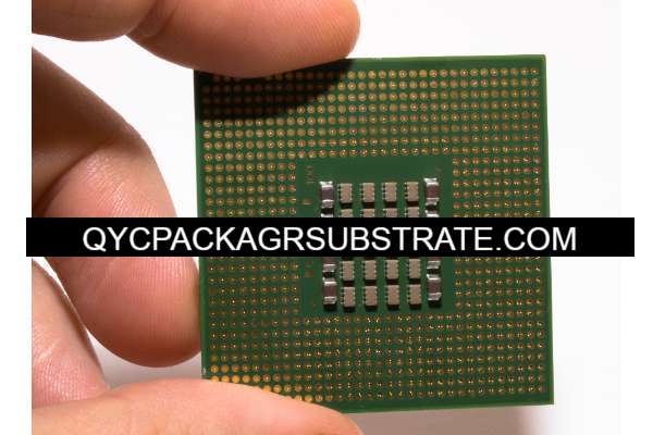
BGA(Ball Grid Array) Packages package substrate provider. Specialized in Msap and Sap production processes, we produce high multi-layer ultra-small trace FC BGA packaging substrates from 4 layers to 20 layers.
Within the constantly evolving realm of electronic components, Ball Grid Array (BGA) packages have risen to prominence. Compact and high-performance packages like BGAs have become essential components in a diverse array of applications, encompassing consumer electronics, industrial machinery, and more. Although the acronym “BGA” might not be widely known, the impact of these packages reaches extensively across various industries.
Brief Overview of BGA (Ball Grid Array) Packages
Ball Grid Array, or BGA for short, is a type of electronic package that has revolutionized the way electronic components are designed and integrated. Unlike traditional pin-grid packages, BGAs use an array of small solder balls to establish electrical connections with a printed circuit board (PCB). This innovative design has allowed for denser and more compact electronic devices, making BGAs a preferred choice for many engineers and manufacturers.
Importance of Substrate Design in Electronic Components
The heart of any electronic component lies within its substrate, a critical but often overlooked element. In the context of BGA packages, the substrate serves as a foundation for the solder balls and a conduit for electrical signals and power delivery. It plays a pivotal role in ensuring the reliability, signal integrity, and thermal performance of the entire package.
Purpose of the Article: To Explore the Rules and Guidelines for BGA Substrate Design
This article delves into the core of BGA substrate design, shedding light on the intricate rules and guidelines that engineers must adhere to when working with these packages. We aim to provide a comprehensive understanding of how a well-designed BGA substrate can make or break the success of an electronic system. From layout considerations to thermal management and signal integrity, this article will equip engineers with the knowledge needed to optimize BGA substrate design and drive innovation in the world of electronics. So, let’s embark on this journey into the world of BGA substrate design and uncover the key principles that can shape the future of electronic components.
Understanding BGA Packages
Explanation of Ball Grid Array (BGA) Packages
Ball Grid Array packages, commonly referred to as BGAs, are a type of integrated circuit packaging.
They consist of a silicon die with solder balls arranged in a grid pattern on the bottom.
The solder balls serve as the electrical and mechanical connection to the circuit board.
BGAs have gained popularity due to their compact design and high pin count.
Key Components of a BGA Package
Silicon Die: The heart of the BGA package, which contains the integrated circuit or semiconductor device.
Solder Balls: The connections between the BGA and the circuit board, providing both electrical and mechanical connections.
Substrate: The layer that holds the silicon die and provides a platform for connecting the die to the solder balls.
Package Cavity: A hollow space beneath the silicon die, often filled with underfill material for protection.
Thermal Interface Material (TIM): Used to manage heat dissipation from the die to the substrate.
Lid or Heat Spreader (Optional): Some BGAs include a heat-spreading component for enhanced thermal management.
Advantages and Applications of BGA Packages
Advantages:
High Density: BGAs offer a high pin count in a compact form factor, allowing more connections in a limited space.
Improved Signal Integrity: Shorter trace lengths and reduced parasitic capacitance and inductance enhance signal quality.
Mechanical Reliability: Solder balls create a strong, reliable mechanical connection to the PCB.
Thermal Performance: Enhanced heat dissipation capabilities due to the direct connection of the die to the PCB.
Reduced Cost: Cost-effective manufacturing processes and efficient use of space.
Applications:
Consumer Electronics: BGAs are used in smartphones, tablets, and laptops due to their small size and high performance.
Networking Equipment: BGA packages are common in routers, switches, and network cards.
Automotive Electronics: Used in engine control units, infotainment systems, and advanced driver-assistance systems.
Aerospace and Defense: BGAs are suitable for harsh environments and are used in avionics and military applications.
Industrial Automation: BGA packages find use in control systems and automation equipment.
In summary, BGA packages are a versatile and efficient packaging solution with widespread applications across various industries, thanks to their numerous advantages, including high pin density, reliability, and superior thermal performance. Understanding the key components of a BGA package is crucial for successful substrate design in electronic systems.
Importance of Substrate in BGA Design
In the realm of BGA (Ball Grid Array) packages, the substrate plays a pivotal role, serving as the unsung hero behind their reliable performance. Let’s delve into the multifaceted significance of substrate design, considering its integral role, impact on overall performance, and the critical aspects of reliability and thermal considerations.
Role of the Substrate in BGA Packages
The substrate, often referred to as the BGA PCB (Printed Circuit Board), acts as the bridge that connects the BGA component to the larger electronic system. It provides the necessary electrical and mechanical connections.
It functions as a central hub, facilitating the transfer of signals and power between the package and the rest of the circuit, making it a vital communication channel.
The substrate also offers mechanical support and protection to the delicate BGA components, ensuring they remain securely in place, even in the face of mechanical stress and temperature fluctuations.
Impact of Substrate Design on Overall Performance
Substrate design profoundly influences the electrical and thermal characteristics of a BGA package. Proper design can optimize signal integrity, minimize signal interference, and enhance the overall system’s speed and performance.
Careful substrate design can lead to reduced electromagnetic interference (EMI) and electromagnetic compatibility (EMC) issues, contributing to the stability of the entire system.
Inadequate substrate design can lead to signal degradation, causing issues like jitter, data errors, and latency, which can be particularly detrimental in high-speed data transmission applications.
Reliability and Thermal Considerations
The reliability of a BGA package heavily depends on the substrate’s ability to withstand environmental stressors. A well-designed substrate minimizes the risk of mechanical failures, such as solder joint fatigue or cracks.
Thermal management is a critical aspect of substrate design, as BGA packages can generate a significant amount of heat during operation. The substrate should include features like thermal vias and heat sinks to dissipate heat effectively, preventing overheating and ensuring long-term reliability.
In addition, the choice of substrate material plays a crucial role in the thermal performance. Materials with high thermal conductivity can help in efficient heat dissipation, enhancing the package’s reliability and lifespan.
In summary, the substrate’s role in BGA design is irreplaceable, as it forms the backbone of the package, impacts its overall performance, and dictates its reliability and thermal behavior. Engineers must pay close attention to substrate design to ensure the success of BGA packages in diverse electronic applications.
Rules for BGA Substrate Design
Layout and Routing Considerations
Efficient layout and routing play a pivotal role in BGA substrate design, ensuring optimal performance and reliability.
Pad Arrangement and Pitch: The arrangement and pitch of the solder pads on the BGA substrate must be carefully planned. Proper pad spacing and alignment are essential to prevent short circuits and enable efficient soldering during assembly.
Escape Routing for Traces: The routing of traces from the BGA to other components demands meticulous attention. Escape routing involves the pathways that connect the inner BGA balls to the outer layers of the board. Routing should be designed to minimize crosstalk and signal interference.
Via Placement and Size: The location and size of vias significantly impact the overall design. Proper via placement is essential for signal and power integrity. Vias should be strategically positioned to minimize signal distortion and ensure efficient thermal dissipation.
Signal Integrity Considerations
Maintaining signal integrity is critical for BGA substrate design, especially in high-speed electronic systems.
Impedance Control: Maintaining consistent impedance across signal traces is crucial. This involves controlling trace widths and layer stackup to match the required impedance, reducing signal reflections and ensuring reliable data transmission.
Crosstalk Prevention: To prevent signal crosstalk (unwanted interference between adjacent traces), proper spacing, shielding, and signal routing techniques must be employed. Crosstalk can degrade signal quality and lead to data errors.
Grounding Techniques: Effective grounding is vital for noise reduction and ensuring a stable reference for signal lines. Employing ground planes, stitching vias, and using a solid ground strategy can minimize ground bounce and improve signal integrity.
Thermal Management
Proper thermal management is crucial to prevent overheating and maintain the reliability of the BGA package.
Thermal Vias and Heat Dissipation: Thermal vias are used to channel heat away from the BGA package and the substrate. Proper placement and size of thermal vias are essential for efficient heat dissipation, preventing thermal stress, and ensuring long-term reliability.
Material Selection for Substrates: The choice of substrate material impacts both electrical and thermal properties. Selecting materials with high thermal conductivity is vital for effective heat dissipation. Careful consideration should be given to material properties, such as coefficient of thermal expansion (CTE), to prevent solder joint failures.
Electrical Considerations
Ensuring reliable power delivery and signal integrity are central to BGA substrate design.
Power Delivery Network Design: Designing a robust power delivery network is critical to supply power to the BGA components. This involves selecting appropriate power plane layers, reducing voltage drops, and ensuring proper distribution of power across the board.
Decoupling Capacitors: Decoupling capacitors play a pivotal role in ensuring stable power distribution and mitigating voltage noise. To preserve signal integrity, it is crucial to carefully position and choose the right decoupling capacitors.
Signal and Power Integrity Analysis: Thorough analysis, including simulations and testing, is crucial to validate the BGA substrate design. This step ensures that the design meets the required signal and power integrity criteria before production, minimizing costly redesigns and improving product quality.
By adhering to these rules for BGA substrate design, engineers can optimize the performance, reliability, and manufacturability of electronic components, meeting the demands of modern technology and applications.
Guidelines for BGA Substrate Design
Once you’ve familiarized yourself with the essential rules for BGA substrate design, it’s crucial to follow these guidelines to ensure a successful outcome and adhere to industry best practices.
Proper Documentation and Design Tools
Comprehensive documentation: Maintain detailed records of your BGA substrate design, including specifications, layouts, and materials used. This documentation aids in troubleshooting and future revisions.
Design software: Utilize advanced PCB design software that supports BGA layout and routing, facilitating accurate component placement and signal integrity analysis.
Revision control: Implement a robust revision control system to track changes and updates to your design, ensuring transparency and traceability.
Testing and Validation Processes
Design verification: Before moving to production, thoroughly verify your BGA substrate design using simulation tools and prototype testing to identify and address potential issues.
Signal integrity testing: Conduct rigorous signal integrity tests to ensure that the high-speed signals within the BGA package meet industry standards and perform optimally.
Thermal testing: Assess the thermal performance of your substrate design to guarantee efficient heat dissipation and prevent overheating issues in the final product.
Reliability testing: Subject your BGA package to reliability tests, such as thermal cycling and mechanical stress tests, to ensure its long-term performance and durability.
Industry Standards and Best Practices
Compliance with industry standards: Familiarize yourself with industry-specific standards like IPC-7095 and IPC-2221 to ensure your BGA substrate design meets universally recognized criteria.
Follow best practices: Stay updated with the latest developments in BGA technology and adhere to best practices recommended by industry experts.
Peer reviews: Engage in peer reviews or seek feedback from experienced professionals to identify potential improvements and ensure your design aligns with industry benchmarks.
Collaboration with Component Manufacturers
Consultation with suppliers: Collaborate closely with BGA component manufacturers to gain insights into their specific requirements and recommendations for your design.
Component availability: Confirm the availability of the chosen BGA components and align their specifications with your design to avoid compatibility issues.
DFM (Design for Manufacturability): Engage with component manufacturers to ensure that your design is manufacturable, considering factors like assembly, soldering, and inspection processes.
By incorporating these guidelines into your BGA substrate design process, you’ll enhance the chances of producing a reliable and high-performance electronic component that adheres to industry standards and best practices. This collaborative and systematic approach will lead to a successful outcome while minimizing potential setbacks.