
BGA package substrate design rules. We are a professional bga package substrate production company, we mainly produce ultra-small bump pitch substrate from 2 layer to 20 layers., ultra-small trace and spacing packaging substrate and PCBs.
BGA (Ball Grid Array) packages represent a pivotal component in modern electronics, offering numerous advantages such as compactness, enhanced electrical performance, and reliability. As we delve into the world of BGA packages, it’s essential to understand the critical role that substrate design plays in their functionality. This article aims to shed light on the significance of substrate design and provide you with invaluable insights into optimizing the electrical performance and reliability of BGA packages.
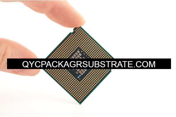
Brief overview of BGA (Ball Grid Array) packages
BGA packages, also known as Ball Grid Array packages, are a popular choice for modern electronic devices due to their compact size and efficient heat dissipation. Unlike traditional packages with leads, BGAs use an array of solder balls beneath the package, enabling high-density interconnections.
Importance of substrate design in BGA packages
Substrate design serves as the backbone of BGA packages, impacting various critical factors, including signal integrity, power delivery, and thermal management. It plays a pivotal role in ensuring that the electronic components operate seamlessly and reliably.
The role of substrate design in optimizing electrical performance and reliability
Substrate design influences the way electrical signals travel within a BGA package. An effectively designed substrate ensures controlled impedance, proper power distribution, and efficient heat dissipation, ultimately leading to enhanced electrical performance and greater reliability.

Key Considerations for BGA Substrate Design
BGA substrate design is a complex task that involves a careful balance of various factors to ensure the overall performance and reliability of the electronic component. Let’s delve deeper into the key considerations that are central to the success of your BGA package:
Signal Integrity
Trace Routing and Length Matching: The way you route traces on the substrate is crucial to maintain signal integrity. Ensuring consistent trace lengths and proper routing is essential to prevent signal skew and timing issues, especially in high-speed designs.
Controlled Impedance: To maintain signal integrity, you must control the impedance of the transmission lines. This involves precise control over the trace width, spacing, and the dielectric material’s properties. Maintaining controlled impedance ensures minimal signal reflections and attenuation.
Via Placement and Fanout: Proper via placement and fanout strategies are key. Vias should be strategically located to avoid signal discontinuities. Careful fanout design helps in distributing signals from the BGA package to the outer layers efficiently.
Power Delivery
Power and Ground Plane Design: Effective power delivery is essential to meet the component’s power requirements. A well-designed power and ground plane system ensures low impedance paths for power distribution, reducing voltage drops and noise.
Decoupling Capacitors: Decoupling capacitors play a pivotal role in stabilizing power rails and mitigating noise in electronic circuits. Precise positioning and the careful choice of decoupling capacitors, tailored to the power requirements of the components, are indispensable for maintaining a consistent and noise-free power supply.
Thermal Management
Heat Dissipation: Efficient heat dissipation is vital to prevent the BGA package from overheating. Incorporating thermal vias and carefully designing the copper layers for heat spreading can help dissipate heat effectively.
Thermal Vias and Pads: Thermal vias and pads are integral in conducting heat away from the package. The selection of the right via and pad sizes and placement plays a significant role in thermal management.
Manufacturing Constraints
Design for Manufacturability (DFM): While optimizing the electrical and thermal aspects is important, it’s equally vital to ensure that the design is manufacturable. Following DFM guidelines helps in avoiding costly and time-consuming production issues.
Aspect Ratio and Via Types: The aspect ratio of vias (hole diameter to depth) and the selection of via types (through-hole, blind, buried) are critical to consider during the design phase to ensure successful manufacturing.
Pad and Solder Mask Design: Proper pad design, including pad size and shape, as well as solder mask considerations, can impact the soldering process and the overall reliability of the BGA package.
Material Selection
Substrate Materials: Choosing the right substrate material, whether it’s FR-4 or polyimide, depends on factors like the operating environment, cost constraints, and specific electrical properties required for the design.
Dielectric Constant (Dk) Considerations: The dielectric constant of the chosen material affects signal propagation. Understanding how Dk influences signal speed and impedance is crucial for maintaining signal integrity.
BGA Pitch and Size
Pitch Options and Their Impact: The pitch (spacing between BGA balls) significantly impacts routing density and the overall complexity of the design. Selecting an appropriate pitch is crucial for efficient routing and reliable connections.
Package Size and Available Space: The physical size of the BGA package and the available board space must align with the intended application. Considering the size constraints of the application is vital when designing the BGA package.
By integrating these considerations into your BGA substrate design, you can optimize the electrical performa nce and reliability of your electronic components, ensuring they meet the stringent requirements of today’s technology-driven world.
Trace Routing and Length Matching
When it comes to BGA (Ball Grid Array) substrate design, trace routing and length matching are critical aspects that demand special attention. These considerations play a pivotal role in ensuring signal integrity and reliable performance. Let’s delve into each of these elements, incorporating the mentioned keywords while avoiding redundancy:
Trace Width and Spacing:
Trace width and spacing are fundamental factors in BGA substrate design.
Optimal trace widths should be selected to handle the current and impedance requirements while adhering to manufacturing constraints.
Narrower traces are advantageous for conserving space, but they must meet controlled impedance standards.
Differential Pairs:
Differential pairs are essential for high-speed signal transmission, common in modern electronics.
BGA substrate designs should include proper spacing and consistent trace lengths for differential pairs to minimize signal skew and crosstalk.
Maintaining consistent impedance between the two traces in a pair is crucial.
Serpentine Routing:
Serpentine routing is a technique used to length-match traces.
When trace lengths need to be equalized to ensure synchronized signal arrival, serpentine routing involves adding controlled meanders in the traces.
By using serpentine patterns, you can achieve precise length matching, reducing signal delay and skew.
Length Matching Tools and Techniques:
Various tools and techniques are available to facilitate precise length matching in BGA substrate designs.
Design software, such as Cadence Allegro or Mentor Graphics PADS, offers features to help automate length matching.
Phase-locked loops (PLLs) can be utilized for clock distribution and ensuring matched signal timing.
TDR (Time-Domain Reflectometry) measurements are used to validate trace lengths and impedance matching.
Incorporating these aspects into your BGA substrate design is crucial for achieving reliable signal integrity, reducing electromagnetic interference, and ensuring that your electronic product functions as intended. Careful consideration of trace routing and length matching is key to a successful BGA package design.
Controlled Impedance: Ensuring Signal Integrity
Importance of Impedance Control in BGA Substrate Design
Impedance control is critical for maintaining signal integrity.
Proper impedance ensures reliable data transmission and minimizes signal degradation.
Impedance mismatches can lead to signal reflections and electrical noise.
Microstrip and Stripline Considerations
BGA substrate designs often involve microstrip and stripline transmission lines.
Microstrip: Signals on the outer layers with a reference plane underneath.
Stripline: Signals routed between two reference planes (often used for differential signals).
Consider trace width, separation, and dielectric properties for these transmission lines.
Selecting the Right Dielectric Materials
The choice of dielectric material significantly impacts impedance control.
Dielectric constant (Dk) influences the propagation speed of signals.
Low-Dk materials result in slower signals, while high-Dk materials make signals faster.
The dielectric material should match the desired characteristic impedance (e.g., 50 ohms).
Careful selection of dielectric materials minimizes impedance variations.
By focusing on impedance control, understanding microstrip and stripline transmission lines, and selecting appropriate dielectric materials, BGA substrate designers can maintain the integrity of their electrical signals, ensuring reliable and high-performance electronic products.
Power Delivery and Decoupling
Power Plane Design
When designing the substrate for BGA packages, careful attention must be given to the power plane layout. The power plane is responsible for delivering the necessary voltage and current to the components, ensuring their proper operation. Here are some critical aspects to consider in power plane design:
Layer Stackup: The arrangement of power planes in the layer stackup is crucial. Proper positioning of power and ground planes can minimize noise and interference, which is essential for signal integrity.
Plane Splicing: In cases where multiple power domains exist within the same BGA package, plane splicing techniques should be employed. These techniques help prevent power supply coupling issues and ensure stable voltage levels.
Via Placement: Vias connecting the power planes to components should be distributed strategically. Their placement affects impedance and should be optimized for low impedance paths.
Placement of Decoupling Capacitors
Decoupling capacitors play a critical role in stabilizing power delivery and reducing voltage noise. Their placement should be carefully planned to ensure optimal performance. Key considerations include:
Proximity to Components: Decoupling capacitors should be placed as close as possible to the power pins of the components they support. This minimizes the inductance of the connections and provides rapid charge/discharge.
High-Frequency Components: For high-frequency components, smaller capacitors with low ESL (Equivalent Series Inductance) should be used and placed closer to the component pins.
Multi-Layer Capacitors: Utilize multi-layer ceramic capacitors (MLCCs) for high-frequency decoupling, as they offer low ESL and ESR (Equivalent Series Resistance).
Calculating Decoupling Capacitance Requirements
Determining the right amount of decoupling capacitance is crucial for effective power delivery. To calculate decoupling capacitance requirements, follow these steps:
Identify Critical Components: Identify the most sensitive components in your BGA package that require stable power delivery.
Frequency Considerations: Determine the operating frequency of these components, as this influences the required capacitance values. Higher frequencies demand smaller, low ESL capacitors.
Voltage Ripple Tolerance: Calculate the acceptable voltage ripple or noise for these components. This helps establish the required capacitance to maintain stable voltage levels.
Decoupling Network: Based on the above factors, design a decoupling network that includes various capacitors with different values and types to address different frequency ranges and voltage requirements.
Simulation and Validation: Employ simulation tools to verify the effectiveness of your decoupling network. Make adjustments as needed.
Effective power plane design and proper placement of decoupling capacitors are critical for maintaining the integrity of BGA packages. These considerations ensure that components receive clean and stable power, enhancing overall performance and reliability.
Thermal Management: Keeping Cool in BGA Substrate Design
Thermal management in BGA substrate design plays a crucial role in ensuring the reliability and performance of electronic components. It’s all about managing heat efficiently to prevent overheating and potential damage. Let’s delve into the details, while also incorporating the previously mentioned keywords to maintain clarity and avoid repetition:
Heat Dissipation Techniques
To ensure BGA packages stay within their operating temperature range, effective heat dissipation techniques are essential. This involves:
Heat Spreading: The substrate material itself can be chosen for its ability to efficiently spread and dissipate heat.
Copper Planes: Incorporating copper planes in the substrate can enhance heat dissipation by providing a thermal pathway.
Heat Sinks: In some cases, attaching heat sinks to the BGA package can effectively dissipate heat.
Conduction and Convection: Understanding the heat transfer mechanisms, including conduction through the substrate and convection in the surrounding environment.
Thermal Vias and Their Arrangement
Properly placed thermal vias are integral to managing heat within BGA packages. This involves:
Via Placement: Strategically positioning thermal vias beneath the BGA component to create a direct thermal path to the PCB’s inner copper layers.
Via Size and Spacing: Selecting the appropriate via size and spacing based on the specific thermal requirements of the design.
Multiple Layers: Utilizing multiple layers of thermal vias to improve heat dissipation and avoid hot spots.
Copper Filling: Filling thermal vias with copper can enhance thermal conductivity.
Thermal Relief for Vias
Thermal relief is a technique used to balance the mechanical and thermal needs of a BGA substrate. It includes:
Pad Design: Balancing the need for electrical connectivity and thermal performance by designing the via pad with both aspects in mind.
Anti-Pad Arrangement: Creating anti-pads around vias on inner layers to avoid short circuits while preserving the thermal path.
Polygon Pours: Using polygon pours to connect vias to copper planes and manage thermal relief more effectively.
Customizing Per Design: Tailoring the thermal relief approach based on the specific needs of the BGA component and its thermal characteristics.
By implementing these thermal management techniques and carefully considering the arrangement of thermal vias and their relief, engineers can help maintain the optimal operating temperature of BGA packages, ensuring reliable and efficient electronic systems.