
BGA Substrate Firm, To use BT(high speed) or Rogers(high frequency). or other types base materials. the microtrace BGA substrates was made in QYC.
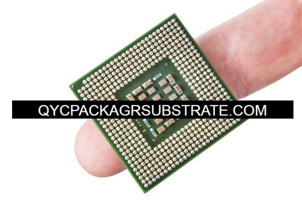
BGA Substrate, or Ball Grid Array Substrate, is a critical element that facilitates the connection between Integrated Circuits (ICs) and other components, characterized by its ball grid array structure. It functions as a type of circuit board typically situated between the chip (IC) and the main circuit board, providing essential connections and support. The primary roles of BGA Substrate include electrical connectivity, signal transmission, and heat dissipation support.
The Ball Grid Array (BGA) is a packaging technology utilized in BGA Substrate, employing small spherical solder balls distributed on the underside of the chip. These solder balls serve to establish connections between the chip and the substrate. The arrangement of these solder balls on the BGA Substrate corresponds to the solder pads on the chip, forming a reliable electrical connection. This structure offers higher density and improved electrical performance compared to traditional surface-mounting technologies.
BGA Substrate finds widespread application in modern electronic devices, particularly in high-performance and high-density applications such as computers, communication equipment, and consumer electronics. Through BGA Substrate, chips can communicate more effectively with other components, while also providing enhanced heat dissipation capabilities to maintain the chip’s stable operating temperature.
What Are the Functions of BGA Substrate?
A BGA (Ball Grid Array) substrate serves several functions, including:
Providing Electrical Connectivity: The BGA substrate facilitates electrical connectivity by using a grid of solder balls to connect the IC chip to the printed circuit board (PCB). This connection method offers higher signal density and improved electrical performance, supporting the high integration of integrated circuits.
Heat Dissipation Support: BGA substrates are often designed with multiple layers, including heat dissipation layers, to efficiently conduct and disperse the heat generated by the IC. This helps to maintain the chip’s temperature within acceptable limits, preventing overheating that could adversely affect device performance and lifespan.
Facilitating High Integration of ICs: The design of BGA substrates allows for the integration of more pins and connections in a smaller physical space, promoting the high integration of integrated circuits. This is crucial for meeting the demands of modern electronic devices for compactness, lightweight design, and high performance.
Providing Mechanical Support: BGA substrates also offer mechanical support to the IC chip, helping prevent chip damage from mechanical stress during use.
In summary, BGA substrates play a crucial role in electrical connectivity, heat dissipation, mechanical support, and overall contribute to being one of the common chip packaging technologies in modern electronic devices.
What Are the Different Types of BGA Substrate?
BGA (Ball Grid Array) substrates come in different types, each with distinct advantages and suitability for various applications. Here are some common types of BGA substrates:
Organic Substrates:
Advantages: Relatively lower cost, simpler manufacturing processes, suitable for most applications.
Applicability: General-purpose BGA substrates, used in a wide range of consumer electronic products.
Inorganic Substrates:
Advantages: Its improved thermal and electrical properties render it highly suitable for high-performance applications.
Applicability: Applied in scenarios demanding elevated performance, like servers and computer processors.
Hybrid Substrates:
Advantages: Merging the advantages of both organic and inorganic substrates, it enhances performance and versatility.
Applicability: Commonly employed in scenarios where both performance and cost factors are crucial.
Multilayer Substrates:
Advantages: Allows for more complex circuit designs, offering higher integration.
Applicability: Suited for applications requiring numerous connections and higher density, such as communication equipment and high-end computing devices.
Film Substrates:
Advantages: Thin and lightweight, suitable for lightweight and portable devices.
Applicability: Commonly employed in situations with constraints on weight and size, such as in portable devices and smartphones.
High-Frequency Substrates:
Advantages: With exceptional high-frequency capabilities, it is ideally suited for applications in RF and microwave technology.
Applicability:Frequently utilized in high-frequency environments like communication, radar, and satellite communication settings.
The choice of BGA substrate depends on the specific requirements of the product, cost considerations, and manufacturing technologies. When selecting a BGA substrate, factors such as electrical performance, thermal performance, mechanical properties, and manufacturing costs need to be carefully considered.
How Does BGA Substrate Differ from PCB?
BGA (Ball Grid Array) substrate and PCB (Printed Circuit Board) are both essential components in electronic design, but they serve different functions within the overall system. Let’s explore the key differences between BGA substrate and PCB to provide a better understanding of their unique roles:
Form and Structure:
PCB: A PCB is a flat board made of insulating material (typically fiberglass) with conductive pathways etched or printed onto its surface. It serves as a platform for mounting and interconnecting various electronic components.
BGA Substrate: BGA substrate, on the other hand, is a specific type of substrate used for packaging integrated circuits (ICs) with a ball grid array configuration. It is a smaller and more specialized component compared to a PCB.
Function:
PCB: The primary function of a PCB is to provide a foundational structure both mechanically and electrically for a wide array of electronic elements, including ICs, resistors, capacitors, and connectors. Its crucial role lies in establishing effective interconnections among these components, thereby creating a fully operational electronic circuit.
BGA Substrate: BGA substrate is specifically designed to house and connect an integrated circuit, usually a microprocessor or other complex ICs. It provides a compact and efficient way to connect the IC to the larger electronic system.
Connection Method:
PCB: Components on a PCB are typically soldered onto the board using surface-mount or through-hole technology. The connections are made through copper traces on the board’s surface.
BGA Substrate: In a BGA package, the IC is mounted on the substrate, and connections are made using an array of tiny solder balls on the underside of the IC. These solder balls form a grid, and they are used for both electrical connections and mechanical attachment.
Density and Miniaturization:
PCB: Printed Circuit Boards (PCBs) are versatile platforms characterized by their larger size, capable of accommodating a diverse array of electronic components with varying dimensions. They find application across a broad spectrum of electronic devices, ranging from simple applications to intricate and complex systems.
BGA Substrate: BGA substrates are tailored for applications that demand high-density circuitry, emphasizing the critical need for miniaturization.The ball grid array configuration allows for a large number of connections in a small space, making it suitable for compact electronic devices.
In summary, while PCBs provide a broad platform for building electronic circuits, BGA substrates are specialized components designed for packaging and connecting high-density integrated circuits. BGA technology is particularly important in modern electronics where space efficiency and miniaturization are key considerations.
What Is the Main Structure and What Are the Production Technologies of BGA Substrate?
A BGA (Ball Grid Array) substrate is an integrated circuit packaging technology primarily used for chip connections in electronic devices. The main structure of a BGA substrate includes several key components:
Substrate Material: The substrate, typically made of glass fiber-reinforced epoxy resin (FR-4), serves as the main body of the BGA. This material possesses good insulation properties and mechanical strength, suitable for electronic device encapsulation.
Trace Layer: The trace layer is a metal wiring layer on the substrate used to connect the pins on the chip and other electronic components. These traces pass through different layers, facilitating signal transmission and connections.
Solder Balls: The bottom of the BGA usually features an array of small ball-shaped solder points used for soldering the BGA to the circuit board. These solder balls are typically made of tin alloy and serve to connect and support the BGA.
Encapsulation Layer: The encapsulation layer covers the top of the substrate, protecting the internal structure from external environmental factors. This layer is typically made of epoxy resin encapsulation material.
High-Density Interconnect (HDI) technology is a crucial technique employed to enhance the efficiency and performance of BGA substrate manufacturing. HDI technology incorporates fine-line and microvia techniques to increase the number of components connected in a limited space. Key aspects include:
Inter-Layer Connection: HDI technology achieves higher circuit density by introducing fine-line and microvia connections between different layers.
Microvia: Microvia refers to smaller circuit connection channels than traditional traces, enabling a more compact arrangement of components on the BGA substrate.
Blind and Buried Via Technology: This technology allows the creation of blind vias and buried vias in internal layers, further increasing circuit connection density.
Thin Core: The use of HDI technology enables the production of thinner BGA substrates, aiding in accommodating more components in limited space.
In summary, the main structure of a BGA substrate includes substrate material, trace layer, solder balls, and encapsulation layer. HDI technology serves as an improved manufacturing method, enhancing connection density and performance through fine-line traces, microvias, and other techniques.
What Are Frequently Asked Questions (FAQs) About BGA Substrate?
What is BGA substrate?
BGA substrate is an electronic packaging technology that involves mounting a set of small ball-shaped solder points beneath a chip to provide higher connection density and improved thermal performance.
What are the applications of BGA substrate in electronic engineering?
BGA substrates are commonly used in integrated circuit packaging, such as microprocessors, chipsets, etc., to enable more compact designs and enhanced thermal management.
What advantages does BGA substrate have over other packaging technologies?
BGA substrates offer higher connection density, shorter signal paths, and better heat dissipation compared to traditional packaging technologies like QFP (Quad Flat Package).
What are the design considerations for BGA substrate?
BGA substrate design involves considerations such as ball layout, interlayer connections, electrical performance, and heat dissipation to ensure reliable performance.
Is the installation and maintenance of BGA substrate more challenging?
Due to solder points being beneath the chip, installing and maintaining BGA substrates may require higher technical expertise and specialized equipment.
What is the difference between BGA substrate and BGA chip?
BGA substrate is the foundational structure that connects the chip, whereas BGA chip refers to a chip packaged using BGA substrate technology. BGA chips are an application of BGA substrates.
How is fault diagnosis and repair performed for BGA substrate?
Fault diagnosis and repair may involve the use of specialized equipment and techniques such as X-ray inspection, infrared thermography, etc.
How does BGA substrate perform in high-temperature environments?
BGA substrates typically perform well in high-temperature environments, but the design needs to consider the thermal stability of materials and employ effective heat dissipation solutions.
What are the future trends in the development of BGA substrate?
With technological advancements, BGA substrates may evolve towards miniaturization, higher integration, and more advanced heat dissipation solutions.
How does the cost of BGA substrate compare to other packaging technologies?
The manufacturing and installation costs of BGA substrates may be higher, but in some applications, the cost difference may be acceptable due to their superior performance.
In Conclusion, How Crucial Is BGA Substrate in Modern Electronic Engineering?
In conclusion, BGA substrate plays a crucial role in modern electronic engineering, making significant contributions to device performance and reliability. BGA (Ball Grid Array) substrate is an electronic packaging technology that connects chips to printed circuit boards (PCBs) by soldering ball-shaped pins on the chip’s bottom side. Here are key aspects highlighting the importance of BGA substrate in contemporary electronic engineering:
High-Density Packaging: BGA substrate achieves high-density packaging through the compact arrangement of small balls, allowing for more pins and connections in limited space.
Superior Thermal Performance: The ball-shaped pins enable more uniform heat dissipation, giving BGA substrate superior thermal performance compared to traditional packaging forms. This is crucial for efficient heat management in high-performance chips in modern electronic devices.
Signal Integrity: BGA substrate, with shorter pin lengths and interconnect distances, enhances the transmission speed and integrity of electrical signals, reducing signal delays and improving overall device performance.
Reliability and Durability: The smaller size of ball-shaped pins soldered at the bottom enhances the resistance to shocks and vibrations, contributing to improved reliability and durability of devices.
Looking ahead, future trends in BGA substrate technology may include:
Higher Density: As electronic devices continue to evolve, there is a growing demand for higher-density packaging. Future BGA substrates may pursue even more compact designs to accommodate the trend toward smaller devices.
Advanced Cooling Techniques: With increasing chip power, there is a rising need for more advanced cooling techniques. Future BGA substrates may integrate innovative cooling solutions to ensure stable temperatures during high-performance operation.
Complex Interconnect Technologies: As device functionalities expand, BGA substrates may adopt more complex interconnect technologies to meet varying application requirements for signal transmission speed and performance.
In summary, BGA substrate is an indispensable component in modern electronic engineering, playing a critical role in enhancing device performance, reliability, and durability. Future developments are likely to drive innovation in BGA substrate technology to meet the dynamic demands of the evolving electronic market.