
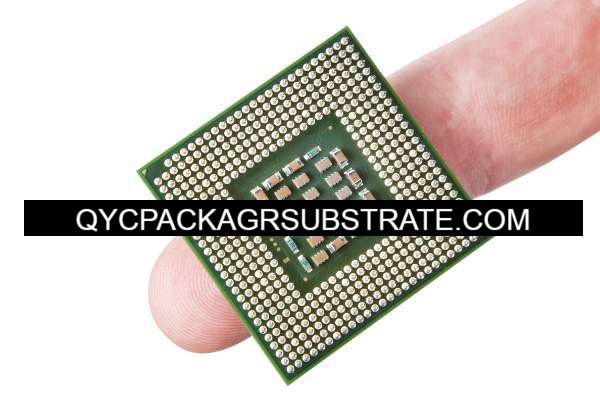
Blind Vias&Buried Vias PCB
Blind Vias&Buried Vias PCB Vendor, the best samllest via holes size are 2mil, and 3mil, the 4mil via holes are common, we use the laser to do the 2mil via holes, our company offer HDI PCBs from 4 layer to 108 layers, Blind vias and buried vias PCB technology represents a significant advancement in printed circuit board design and manufacturing. These innovative techniques enable the creation of highly compact and complex electronic devices by facilitating connections between different layers of the PCB without traversing the entire thickness of the board.
Blind vias extend from the outer layer(s) of the PCB to one or more inner layers, stopping partway through the board, while buried vias exist entirely within the inner layers, connecting them without any external visibility. By utilizing blind and buried vias, designers can achieve higher routing densities, reduced signal distortion, and improved signal integrity, making them ideal for applications requiring miniaturization and high-performance electronics.
Despite their complexity, blind vias and buried vias offer significant benefits such as increased design flexibility, enhanced reliability, and improved thermal management. However, their implementation requires careful consideration of factors like layer stackup, via aspect ratio, and fabrication costs. Overall, blind vias and buried vias PCB technology opens up new possibilities for creating smaller, more efficient electronic devices across various industries.
What is a Blind Vias&Buried Vias PCB?
Blind Vias&Buried Vias PCB manufacturing and package substrate manufacturing. We use advanced Msap and Sap technology, High multilayer interconnection substrates from 4 to 18 layers,
Blind vias and buried vias are specialized types of vias used in printed circuit boards (PCBs) to enable connections between different layers of the board.
- Blind Vias: Blind vias are vias that connect the outer layer(s) of a PCB to one or more inner layers, but do not penetrate through the entire board. Instead, they only extend partway through the PCB, terminating at one of the inner layers. This allows for connections between specific outer-layer traces and inner-layer traces without passing through the entire thickness of the board. Blind vias are commonly used in multilayer PCBs where space is limited, and routing traces directly between outer and inner layers is necessary.
- Buried Vias: Buried vias are similar to blind vias in that they connect one or more inner layers of a PCB, but they do not extend to any outer layers. Instead, they exist entirely within the inner layers of the PCB, providing connections between inner-layer traces without any external visibility. Buried vias are often used when high-density interconnections are needed between inner layers of a PCB, without affecting the outer layer routing or requiring additional drilling through outer layers.
Both blind vias and buried vias are advanced PCB manufacturing techniques that allow for greater flexibility in routing traces and interconnecting components in multilayer PCB designs. They are particularly useful in high-density and high-performance electronic devices where space is limited and signal integrity is critical. However, the use of blind and buried vias adds complexity and cost to the PCB manufacturing process compared to traditional through-hole vias that penetrate the entire thickness of the board.
Blind Vias&Buried Vias PCB manufacturing
What are the Blind Vias&Buried Vias PCB Design Guidelines?
Here are some general guidelines for designing PCBs with blind vias and buried vias:
- Layer Stackup Design: Plan the layer stackup carefully to accommodate blind and buried vias. Ensure that the necessary inner layers are available for routing and that there’s sufficient space between layers to accommodate the vias without causing signal integrity issues.
- Minimum Annular Ring and Pad Size: Maintain appropriate annular ring and pad sizes for blind and buried vias to ensure reliable connections and manufacturability. Consult your PCB manufacturer for specific recommendations based on their capabilities.
- Aspect Ratio: Consider the aspect ratio of the vias, which is the ratio of the via’s length to its diameter. High aspect ratios can make plating and drilling more challenging. Keep the aspect ratio within manufacturable limits, typically around 8:1 or lower, depending on the PCB fabrication process.
- Via Clearance: Provide adequate clearance between vias, traces, and other elements to prevent electrical shorts or manufacturing issues. Ensure that the design meets the minimum clearance requirements specified by your PCB manufacturer.
- Placement and Routing: Place blind and buried vias strategically to optimize signal integrity, minimize signal reflections, and reduce impedance mismatches. Route critical signals on layers that can be accessed using blind vias or buried vias to minimize signal distortion.
- Design Rule Checks (DRC): Perform thorough design rule checks to identify any violations related to blind and buried vias, such as minimum pitch, annular ring, and clearance violations. Address any DRC errors before proceeding with manufacturing.
- Testing and Validation: Validate the design using simulations or prototypes to ensure that blind and buried vias meet performance requirements and do not introduce signal integrity issues. Conduct signal integrity analysis to verify impedance control and minimize reflections.
- Communication with PCB Manufacturer: Communicate clearly with your PCB manufacturer regarding the use of blind and buried vias, specifying the design requirements and any specific manufacturing constraints. Collaborate with them to optimize the design for manufacturability and reliability.
By following these guidelines, you can design PCBs with blind vias and buried vias that meet performance requirements while ensuring manufacturability and reliability.
What is the Blind Vias&Buried Vias PCB Fabrication Process?
The fabrication process for PCBs with blind vias and buried vias involves several steps, including:
- Design Preparation: The process begins with the design of the PCB layout, including the placement of components, routing of traces, and specification of blind and buried vias in the design files. Design software is used to create the layout according to the specific requirements of the PCB.
- Layer Stackup: Based on the design requirements, a layer stackup is determined, specifying the arrangement and sequence of copper layers and insulating layers. This stackup considers the location of blind and buried vias within the PCB structure.
- Drilling: Holes for blind vias and buried vias are drilled into the PCB substrate using precision drilling equipment. For blind vias, the drilling process only penetrates partway through the PCB, while buried vias are drilled entirely within the inner layers.
- Electroless Copper Deposition: After drilling, the walls of the vias are coated with a thin layer of electroless copper to promote adhesion and conductivity. This process involves immersing the PCB in a chemical bath containing a solution of copper ions.
- Copper Plating: The entire surface of the PCB is then plated with a thicker layer of copper through an electroplating process. This adds copper to the walls of the vias as well as the surface of the PCB, forming the conductive traces and connections.
- Lamination: Multiple layers of pre-preg (pre-impregnated resin) and copper foil are stacked together according to the layer stackup design. The stack is then pressed and heated under pressure to bond the layers together, forming a solid PCB substrate.
- Circuit Patterning: A photoresist layer is applied to the surface of the PCB, and the desired circuit patterns are transferred onto the photoresist using a photolithography process. The exposed areas of the photoresist are then chemically etched away, leaving behind the desired copper traces.
- Final Finishing: The PCB is subjected to final finishing processes, such as surface treatment (e.g., HASL, ENIG, OSP) and solder mask application. These processes protect the copper traces, provide solderability, and improve the overall reliability of the PCB.
- Testing and Inspection: The finished PCB undergoes thorough testing and inspection to ensure that it meets the required specifications and quality standards. This may include electrical testing, visual inspection, and other quality control measures.
- Assembly: Once the PCBs pass inspection, they are ready for component assembly, where electronic components are soldered onto the board to create the final electronic product.
Throughout the entire fabrication process, careful attention is paid to the precise control of dimensions, materials, and manufacturing parameters to ensure the reliability and performance of the PCB with blind and buried vias.
How do you manufacture a Blind Vias&Buried Vias PCB?
Manufacturing a PCB with blind vias and buried vias involves several specialized steps in the fabrication process. Here’s an overview of the typical process:
- Design Preparation: The process starts with the PCB design, where the designer specifies the locations of blind vias and buried vias in the layout. Design software is used to create the PCB layout with these vias included.
- Layer Stackup: The PCB manufacturer creates a layer stackup based on the design requirements. This stackup defines the arrangement and thickness of the copper and dielectric layers in the PCB.
- Drilling: The first step in manufacturing blind and buried vias involves drilling holes in the PCB substrate. For blind vias, these holes only penetrate partway through the board, while buried vias are drilled entirely within the inner layers. Advanced drilling techniques, such as laser drilling or mechanical drilling with controlled depth, are used for precision.
- Electroless Copper Deposition: After drilling, the walls of the vias are plated with a thin layer of electroless copper to improve conductivity and facilitate subsequent plating processes.
- Layer Lamination: The drilled panels are then laminated together with prepreg and copper foil to form a solid multilayer structure. This process encases the buried vias within the inner layers of the PCB.
- Plating: Copper plating is performed to fill the vias and create electrical connections between the layers. For blind vias, a plating process is used to selectively plate copper inside the vias, stopping at the desired depth. Buried vias are filled entirely during this process.
- Outer Layer Processing: After plating, outer layer processing is carried out to create circuit traces, solder mask application, and surface finish deposition on the outer layers of the PCB.
- Final Finishing: The PCB undergoes final finishing processes, including etching excess copper, applying silkscreen legend, and routing individual boards from the panel.
- Quality Control and Testing: Throughout the fabrication process, quality control measures are implemented to ensure that the PCB meets design specifications. Testing may include checks for dimensional accuracy, electrical continuity, and signal integrity.
- Assembly: Once the PCBs are manufactured, they can be assembled with electronic components to create functional electronic devices.
Manufacturing PCBs with blind and buried vias requires specialized equipment and expertise to ensure precise drilling, plating, and lamination processes. Collaboration between PCB designers and manufacturers is essential to optimize the design for manufacturability and reliability.
How much should a Blind Vias&Buried Vias PCB cost?
The cost of a PCB with blind vias and buried vias can vary significantly depending on several factors:
- Board Size: Larger PCBs generally cost more due to the increased material and manufacturing expenses.
- Layer Count: Multilayer PCBs with blind and buried vias typically cost more than single or double-layer boards because of the additional layers and complexity involved in fabrication.
- Materials: The choice of materials, such as substrate material (FR-4, Rogers, etc.) and copper thickness, can impact the cost.
- Complexity of Design: PCBs with intricate layouts, dense component placement, and high-speed signal routing may require more advanced manufacturing processes, driving up the cost.
- Quantity: Economies of scale apply – larger production runs usually result in lower per-unit costs.
- Manufacturing Technology: The specific fabrication techniques and equipment required for blind and buried vias can influence the cost.
- Turnaround Time: Expedited manufacturing services typically come at a premium compared to standard lead times.
- Additional Services: Extra services such as impedance control, gold plating, and specialty surface finishes may increase the overall cost.
To obtain an accurate cost estimate for a PCB with blind and buried vias, it’s best to consult with PCB manufacturers directly. They can provide quotes based on your specific design requirements, including factors such as board size, layer count, materials, and desired quantity. Additionally, consider obtaining quotes from multiple manufacturers to compare prices and services offered.
What is Blind Vias&Buried Vias PCB base material?
The base material for PCBs with blind vias and buried vias is typically similar to that of standard multilayer PCBs. The most common base material used for PCBs includes:
- FR-4 (Flame Retardant 4): FR-4 is a widely used substrate material for PCBs due to its affordability, mechanical strength, and good electrical properties. It consists of woven fiberglass cloth impregnated with epoxy resin.
- High-Temperature FR-4: For applications requiring higher thermal performance, high-temperature FR-4 variants are available. These materials have increased glass transition temperatures (Tg), which make them suitable for use in environments with elevated temperatures.
- Rogers Materials: Rogers Corporation produces a range of high-performance laminates suitable for demanding applications. These materials offer excellent electrical properties, low loss tangents, and stable dielectric constants across a wide frequency range.
- Polyimide: Polyimide substrates, such as Kapton, are used in applications requiring flexibility or resistance to high temperatures. They are commonly used in flexible PCBs and rigid-flex PCBs.
The choice of base material depends on various factors such as thermal requirements, electrical properties, cost considerations, and the specific demands of the application. Regardless of the base material chosen, it’s essential to ensure that it meets the required specifications for the intended use of the PCB, including compatibility with the manufacturing processes involved in creating blind and buried vias.
Which company makes Blind Vias&Buried Vias PCB?
Many PCB manufacturing companies are capable of producing PCBs with blind vias and buried vias. These companies have advanced manufacturing equipment and technology to meet the specific needs of customers. PCB manufacturers around the world offer services with this advanced technology, including well-known companies such as Foxconn, JLCPCB, Goedrum, Optimum, Samsung Electro-Mechanics, and Hitachi Chemical. These companies possess extensive experience and expertise to provide high-quality PCB products with blind vias and buried vias.
As for our company, we are also a professional PCB manufacturer with advanced production equipment and a skilled technical team. We prioritize quality and customer satisfaction and have rich experience in manufacturing PCBs with blind vias and buried vias. Our manufacturing processes ensure the accuracy and reliability of blind and buried vias, meeting the demand for high-quality PCBs from our customers.
We have an experienced team capable of customizing PCBs with blind vias and buried vias according to the specific requirements of customers, offering personalized solutions. We emphasize communication and collaboration with customers, striving to understand their needs and provide the best solutions. With our expertise and professional services, we ensure to deliver high-quality, reliable PCB products with blind vias and buried vias to our customers.
In conclusion, many well-known PCB manufacturers can produce PCBs with blind vias and buried vias, including Foxconn, JLCPCB, Goedrum, and others. Our company is among them, equipped with advanced manufacturing equipment and extensive experience, capable of providing high-quality custom PCBs with blind vias and buried vias to meet our customers’ needs.
What are the 7 qualities of good customer service?
Good customer service is characterized by several key qualities that contribute to positive experiences for customers. Here are seven qualities often associated with excellent customer service:
- Responsiveness: Promptly addressing customer inquiries, concerns, or issues demonstrates responsiveness. Whether it’s answering questions, resolving problems, or providing assistance, being readily available and proactive in communication shows customers that their needs are valued.
- Empathy: Showing empathy involves understanding and acknowledging the customer’s feelings, concerns, and perspectives. Empathetic responses demonstrate that the company cares about the customer’s experience and is genuinely committed to helping them find solutions to their problems.
- Clear Communication: Effective communication is essential for providing good customer service. It involves conveying information clearly and concisely, using language that the customer can understand. Clear communication helps prevent misunderstandings and ensures that customers receive accurate and helpful assistance.
- Knowledgeability: Customer service representatives should possess thorough knowledge of the company’s products, services, policies, and procedures. Being knowledgeable allows them to answer questions accurately, provide relevant information, and offer appropriate solutions to customer issues or inquiries.
- Professionalism: Maintaining a professional demeanor and attitude is crucial in all interactions with customers. This includes being courteous, respectful, and attentive while remaining calm and composed, even in challenging situations. Professionalism builds trust and confidence in the company’s ability to meet the customer’s needs.
- Problem-Solving Skills: Effective problem-solving skills are essential for resolving customer issues efficiently and satisfactorily. Customer service representatives should be able to identify the root cause of problems, explore various solutions, and implement strategies to address the customer’s concerns effectively.
- Consistency: Consistency in service delivery ensures that customers receive a uniform and reliable experience each time they interact with the company. Consistent service standards, policies, and procedures help build trust and loyalty by setting clear expectations for customers and delivering on promises consistently.
By embodying these qualities, organizations can establish strong relationships with their customers, foster loyalty, and differentiate themselves in competitive markets through exceptional customer service.
FAQs
What are blind vias and buried vias?
Blind vias are holes that connect the outer layer(s) of a PCB to one or more inner layers, without penetrating the entire board. Buried vias are similar but exist entirely within the inner layers, connecting one or more of these layers without extending to any outer layers.
What are the advantages of using blind and buried vias?
Blind and buried vias enable high-density interconnections in multilayer PCBs, allowing for more compact and complex designs. They also reduce signal distortion and improve signal integrity by minimizing the length of signal paths.
What are the typical applications of blind and buried vias PCBs?
Blind and buried vias are commonly used in high-density electronic devices such as smartphones, tablets, laptops, and other portable electronics. They are also utilized in networking equipment, aerospace systems, and high-performance computing applications.
How do blind and buried vias affect PCB fabrication costs?
PCBs with blind and buried vias generally incur higher manufacturing costs compared to traditional through-hole vias. The additional fabrication steps and specialized equipment required for drilling and plating these vias contribute to the increased cost.
What design considerations are important when using blind and buried vias?
Designers must consider factors such as layer stackup, via aspect ratio, minimum annular ring and pad size, clearance requirements, and signal routing strategies to optimize the use of blind and buried vias while ensuring manufacturability and signal integrity.
Can blind and buried vias be used together with other via types?
Yes, blind and buried vias can be used in conjunction with through-hole vias and other advanced via types such as microvias. Designers often employ a combination of via types to achieve the desired routing density and signal performance in complex PCB designs.
What are the limitations or challenges associated with blind and buried vias?
Blind and buried vias may pose challenges in terms of fabrication complexity, increased lead times, and limited design flexibility compared to traditional via types. Additionally, controlling impedance and ensuring reliable plating can be more challenging with blind and buried vias.