
Buried Cavity Package Substrate Manufacturer
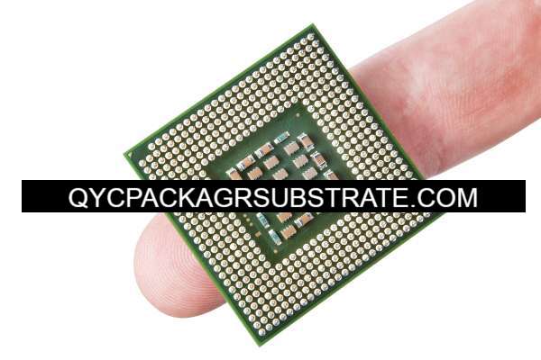
Buried Cavity Package Substrate Manufacturer,Buried Cavity Package Substrates are advanced PCBs designed with internal recesses or cavities that are encapsulated within the substrate layers. These cavities can house sensitive components such as semiconductor chips or passive devices, providing protection against environmental factors and enhancing electrical performance. By embedding components within the substrate, Buried Cavity Package Substrates reduce the overall profile of the package, optimize signal integrity, and improve thermal management. They are ideal for applications requiring compact and reliable electronic packaging solutions, such as aerospace, automotive electronics, and telecommunications. These substrates are engineered with precision to ensure robustness, reliability, and efficient operation in demanding environments.
What is a Buried Cavity Package Substrate?
A Buried Cavity Package Substrate is an advanced semiconductor packaging technology designed to enhance the performance and reliability of electronic components. This packaging technique involves creating one or multiple buried cavities within the substrate, allowing components to be embedded inside. This reduces the overall thickness and size of the package, which is crucial for high-density integration and miniaturization in electronic products.
The manufacturing process of a buried cavity package substrate typically involves multi-layer substrate stacking. Precision etching techniques are used to form the required cavity structures within single or multiple layers of the substrate. These cavities are then enclosed through lamination and bonding processes to form a complete multi-layer substrate. Within this packaging substrate, cavities can accommodate various electronic components such as integrated circuit chips, capacitors, and inductors, shielding them from external environmental factors.
Buried cavity package substrates offer several advantages. They significantly reduce package thickness and weight, particularly beneficial for mobile devices and portable electronics. By burying sensitive electronic components inside the substrate, they provide better electromagnetic shielding, reducing noise interference and improving signal integrity. Additionally, buried cavity package substrates enhance thermal management by optimizing heat dissipation paths, thereby extending component lifespan.
This packaging technology finds wide application in high-performance computing, communication devices, medical electronics, aerospace, and other fields. As electronic products continue to trend towards higher integration and smaller sizes, buried cavity package substrates are expected to play an increasingly critical role in the future.
Buried Cavity Package Substrate Manufacturer
What are the Buried Cavity Package Substrate Design Guidelines?
Design guidelines for Buried Cavity Package Substrates focus on several key aspects to ensure optimal performance and reliability:
- Cavity Design and Placement:Designers must carefully plan the size, shape, and placement of cavities within the substrate. This includes considerations for the number of cavities, their dimensions relative to the components to be housed, and their positioning to optimize signal paths and thermal management.
- Substrate Material Selection: Choosing suitable substrate materials is crucial. These materials should have excellent dielectric properties to minimize signal loss and crosstalk. They should also facilitate effective heat dissipation to maintain component reliability.
- Layer Stackup and Routing:The substrate’s layer stackup and routing play a critical role in achieving electrical performance. Designers need to optimize the layer configuration to minimize impedance variations and ensure signal integrity across the substrate.
- Thermal Management:Efficient thermal management is essential to prevent overheating of embedded components. Design guidelines include provisions for thermal vias, thermal pads, and substrate materials with high thermal conductivity to dissipate heat effectively.
- EMI/EMC Considerations:Buried cavity substrates should be designed to mitigate electromagnetic interference (EMI) and ensure electromagnetic compatibility (EMC). This involves incorporating shielding techniques and optimizing the layout to minimize noise coupling.
- Manufacturability and Assembly:Designs should be manufacturable within acceptable tolerances and compatible with assembly processes. This includes considerations for lamination processes, bonding techniques, and handling of multiple layers during fabrication.
- Reliability and Testing: Designers should anticipate reliability challenges such as stress on interconnects, thermal cycling effects, and mechanical stability. Guidelines may include recommendations for testing procedures to validate substrate performance under operating conditions.
- Cost Efficiency: While optimizing performance, designers also consider cost-effective solutions. This involves balancing material choices, manufacturing complexity, and assembly processes to achieve the desired performance at a competitive cost.
By adhering to these design guidelines, engineers can develop Buried Cavity Package Substrates that meet stringent performance requirements for various applications in electronics, telecommunications, automotive, and other industries.
What is the Buried Cavity Package Substrate Fabrication Process?
The fabrication process of a Buried Cavity Package Substrate involves several intricate steps to create the substrate with embedded cavities for housing electronic components. Here is an overview of the typical fabrication process:
- Substrate Selection:Choose a suitable substrate material based on the application requirements, such as dielectric constant, thermal conductivity, and mechanical strength. Common materials include various types of high-frequency laminates or ceramics.
- Layer Preparation:Prepare multiple layers of substrate material. Each layer is typically coated with a thin layer of copper on both sides to facilitate circuitry and interconnection.
- Cavity Formation:Use precision etching techniques to create cavities within the substrate layers. This involves selectively removing substrate material to form the desired cavity shapes and sizes. The cavities are strategically located according to the design requirements for component placement and signal routing.
- Layer Alignment and Lamination: Stack the prepared substrate layers together, ensuring precise alignment of the cavities across all layers. The layers are then laminated under heat and pressure to bond them together into a single multi-layer substrate. This step also involves the curing of the resin used in the substrate material.
- Cavity Enclosure:Once the layers are laminated, the cavities need to be enclosed to form sealed compartments. This can be achieved through several methods, including the use of cover layers with matching cutouts, bonding films, or additional lamination cycles with appropriate materials.
- Copper Circuit Patterning:Apply a photoresist layer and use photolithography to define copper circuit patterns on the substrate surfaces. This process includes etching away unwanted copper and leaving behind the desired conductive traces that connect the components inside the cavities.
- Surface Finish:Apply a surface finish to the substrate to protect the copper traces and provide solderability for component attachment during assembly. Common surface finishes include electroless nickel immersion gold (ENIG) or organic solderability preservatives (OSP).
- Quality Control and Testing:Conduct thorough quality control checks throughout the fabrication process. This includes dimensional inspections of cavities, electrical testing of circuit integrity, and verification of substrate flatness and layer alignment.
- Assembly Compatibility:Ensure that the finished substrate design is compatible with subsequent assembly processes. This involves consideration of solder mask application, via filling, and any additional components that may be mounted on the substrate surface or within the cavities.
- Final Inspection and Packaging:Perform final inspection procedures to confirm that the fabricated Buried Cavity Package Substrates meet all specified requirements for functionality, reliability, and performance. Substrates are then packaged and prepared for shipment to assembly facilities.
By following these fabrication steps with precision and attention to detail, manufacturers can produce Buried Cavity Package Substrates that meet the stringent demands of modern electronic applications, including telecommunications, aerospace, and high-performance computing.
How do you manufacture a Buried Cavity Package Substrate?
Manufacturing a Buried Cavity Package Substrate involves a detailed and precise process to create a substrate with embedded cavities for housing electronic components. Here’s a step-by-step outline of the typical manufacturing process:
- Substrate Material Selection:Choose a substrate material that meets the specific requirements of the application, such as high-frequency laminates or ceramics with appropriate dielectric constants, thermal conductivity, and mechanical properties.
- Layer Preparation:Prepare multiple layers of substrate material. Each layer is typically coated with a thin layer of copper on both sides to facilitate circuitry and interconnection.
- Cavity Design and Formation:Design the layout and dimensions of cavities based on the placement and size requirements of electronic components. Use precision etching techniques or laser drilling to selectively remove substrate material and form the cavities within each substrate layer.
- Layer Alignment and Lamination:Stack the prepared substrate layers together in the desired order, ensuring precise alignment of the cavities across all layers. The layers are then laminated under heat and pressure to bond them together into a single multi-layer substrate. This process also involves curing the resin used in the substrate material.
- Cavity Enclosure:Once the layers are laminated, the cavities need to be enclosed to form sealed compartments. This can be achieved by applying cover layers with matching cutouts, bonding films, or additional lamination cycles using materials that provide effective sealing.
- Copper Circuit Patterning:Apply a photoresist layer to the substrate surfaces and use photolithography techniques to define copper circuit patterns. Etch away unwanted copper using chemical processes, leaving behind the desired conductive traces that connect components inside the cavities.
- Surface Finish:Apply a surface finish to the substrate to protect the copper traces and ensure solderability for component attachment during assembly. Common surface finishes include electroless nickel immersion gold (ENIG) or organic solderability preservatives (OSP).
- Quality Control and Testing:Conduct rigorous quality control checks throughout the manufacturing process. This includes dimensional inspections of cavities, electrical testing of circuit integrity, and verification of substrate flatness and layer alignment.
- Assembly Compatibility:Ensure that the finished substrate design is compatible with subsequent assembly processes. This involves considerations such as solder mask application, via filling, and the mounting of additional components on the substrate surface or within the cavities.
- Final Inspection and Packaging:Perform final inspection procedures to confirm that the manufactured Buried Cavity Package Substrates meet all specified requirements for functionality, reliability, and performance. Substrates are then packaged and prepared for shipment to assembly facilities.
By following these steps with precision and attention to detail, manufacturers can produce Buried Cavity Package Substrates that meet the stringent demands of modern electronic applications, ensuring high performance, reliability, and miniaturization capabilities.
How much should a Buried Cavity Package Substrate cost?
The cost of a Buried Cavity Package Substrate can vary widely depending on several factors:
- Substrate Material:The type and quality of substrate material used (e.g., high-frequency laminates, ceramics) significantly impact cost.
- Number of Layers:More layers typically increase manufacturing complexity and cost.
- Cavity Complexity:The number, size, and complexity of cavities affect fabrication time and material usage.
- Design Complexity:Intricate circuit designs and tight tolerances may increase costs due to more precise manufacturing requirements.
- Surface Finish:Different surface finishes (e.g., ENIG, OSP) have varying costs and impact assembly processes.
- Quantity:Economies of scale apply; larger quantities usually reduce per-unit costs due to bulk production efficiencies.
- Manufacturing Location:Costs can vary based on labor rates, manufacturing capabilities, and overhead expenses in different regions.
Given these variables, it’s challenging to provide a specific cost without detailed specifications. Generally, Buried Cavity Package Substrates are considered premium products due to their advanced manufacturing processes and specialized requirements. Prices can range from several dollars to tens or even hundreds of dollars per substrate, depending on the factors mentioned above and the specific application requirements. For precise cost estimates, it’s advisable to consult with substrate manufacturers who can provide quotes based on detailed design specifications and production volumes.
What is Buried Cavity Package Substrate base material?
The base materials used for Buried Cavity Package Substrates vary depending on the specific requirements of the application. However, commonly used materials include:
- High-Frequency Laminates: These laminates are designed to have low dielectric constants and low loss tangents at high frequencies, making them suitable for applications requiring excellent signal integrity.
- Ceramics:Certain types of ceramics are chosen for their high thermal conductivity and excellent mechanical stability, which are crucial for applications needing efficient heat dissipation and robust structural support.
- Advanced Composite Materials:Some substrates combine fiberglass with epoxy resins or other advanced materials to achieve a balance of electrical performance, mechanical strength, and cost-effectiveness.
The choice of base material depends on factors such as operating frequency, thermal management requirements, mechanical strength, and cost considerations. Each material type offers different advantages, and the selection is tailored to meet the specific performance and reliability demands of Buried Cavity Package Substrate applications in industries like telecommunications, aerospace, and high-performance computing.
Which company makes Buried Cavity Package Substrates?
Currently, there are several companies manufacturing Buried Cavity Package Substrates, each with extensive applications and technological expertise in the field of electronic component packaging. Some notable international companies include Materion from the United States, Sumitomo Chemical from China, Nippon Steel & Sumitomo Metal Corporation from Japan, and Silicon Alloys from South Korea.
Buried Cavity Package Substrates, as an advanced semiconductor packaging technology, are primarily used in electronic products requiring high performance and miniaturization, such as communication equipment, aerospace systems, medical electronics, and more. The development of this technology demands excellent electrical properties and thermal management capabilities in material selection, as well as precision and reliability in manufacturing processes.
Our company is also capable of producing Buried Cavity Package Substrates, leveraging the following advantages and capabilities:
- Advanced Manufacturing Facilities and Technology:We possess advanced production facilities and a skilled technical team capable of meeting complex multi-layer substrate manufacturing requirements to ensure high-quality production.
- Rich Experience and Expertise:Our team has extensive experience and expertise in the semiconductor packaging field, enabling us to customize designs and produce Buried Cavity Package Substrates that meet high standards and specific customer requirements.
- Comprehensive Quality Control and Testing:We implement stringent quality control measures, monitoring and testing every step from material selection to manufacturing processes to ensure products meet customer requirements and expectations.
- Customer Customization and Support:We provide personalized product customization services, designing and manufacturing products tailored to specific customer application needs. We also offer professional technical support and after-sales service to ensure customer satisfaction and foster long-term partnerships.
Therefore, if your company has a demand for Buried Cavity Package Substrates or any related inquiries, we are ready to provide assistance and discuss how we can meet your specific application requirements.
What are the 7 qualities of good customer service?
Good customer service is characterized by several key qualities that contribute to a positive customer experience and foster customer loyalty. Here are seven qualities of good customer service:
- Responsiveness:Promptly addressing customer inquiries, concerns, and requests demonstrates respect for their time and needs. Responding in a timely manner helps to build trust and satisfaction.
- Empathy:Understanding and empathizing with customers’ perspectives and emotions shows that you care about their experience. Empathetic responses can diffuse tensions and strengthen rapport.
- Clear Communication:Communicating clearly and effectively ensures that customers understand information, instructions, and solutions. Avoiding jargon and using plain language helps to prevent misunderstandings.
- Problem-Solving Skills:Effectively resolving issues and finding solutions that meet customer needs demonstrates competence and commitment to customer satisfaction. Problem-solving skills are crucial for turning negative experiences into positive ones.
- Professionalism:Maintaining a professional demeanor, whether in person, over the phone, or online, instills confidence and reassurance in customers. Professionalism includes being courteous, respectful, and maintaining confidentiality.
- Adaptability:Being flexible and adaptable to different customer preferences and situations shows a willingness to accommodate varying needs. Adaptability helps in providing personalized service and addressing unique customer requirements.
- Follow-Up:Following up with customers after resolving an issue or completing a transaction shows appreciation and ensures satisfaction. Following up can also gather feedback for continuous improvement and strengthen customer relationships.
By embodying these qualities consistently, businesses can enhance their reputation, build customer loyalty, and differentiate themselves in competitive markets.
FAQs about Buried Cavity Package Substrates
What are Buried Cavity Package Substrates?
Buried Cavity Package Substrates are advanced semiconductor packaging technologies that involve creating embedded cavities within the substrate. These cavities can house electronic components like integrated circuits, providing benefits such as reduced package size and improved thermal management.
What are the benefits of Buried Cavity Package Substrates?
Benefits include enhanced miniaturization, improved electrical performance due to reduced parasitics, better thermal management capabilities, and increased reliability by protecting sensitive components from external environmental factors.
Where are Buried Cavity Package Substrates used?
They are used in various high-performance electronic applications such as telecommunications equipment, aerospace systems, medical devices, and high-speed computing where compact size, high reliability, and efficient heat dissipation are critical.
How are Buried Cavity Package Substrates manufactured?
Manufacturing involves several steps including substrate material selection, layer preparation, cavity formation using precision etching or drilling, lamination of layers to form a multi-layer substrate, enclosure of cavities, copper circuit patterning, surface finishing, and rigorous quality control.
What types of materials are used for Buried Cavity Package Substrates?
Common materials include high-frequency laminates, ceramics with high thermal conductivity, and advanced composite materials. These materials are chosen based on specific application requirements for electrical properties, mechanical strength, and thermal management.
What are the considerations for designing Buried Cavity Package Substrates?
Design considerations include cavity placement and dimensions, substrate material selection, thermal management strategies, electrical performance optimization, and ensuring compatibility with assembly processes.
Who manufactures Buried Cavity Package Substrates?
Several companies globally specialize in manufacturing Buried Cavity Package Substrates, providing customized solutions tailored to specific application needs in various industries requiring high-performance electronic packaging.