
Cavity PCB| High Speed PCB Manufacturer
Cavity PCB Vendor, Open Cavity on the PCBs. It is very important to control the depth and size of the Cavity by putting components into the Cavity area. We have produced many such Cavity PCBs,, some of which have only one Cavity per unit, and some of which have many such designs, or embedded Cavity we can produce them too. we can use the High Speed and High-frequency material.
Cavity PCBs, also known as cavity printed circuit boards, represent an innovative approach to electronic circuit design and manufacturing. These PCBs feature recessed sections or “cavities” within the board itself, serving various purposes such as housing components, providing shielding, or improving thermal management. By integrating components into the board structure, cavity PCBs enable more compact and efficient electronic devices while ensuring reliable performance and protection against external influences.
The design process for cavity PCBs involves careful consideration of factors such as component placement, cavity dimensions, material selection, EMI shielding, thermal management, and manufacturability. Engineers strive to optimize these parameters to meet the specific requirements of the application while adhering to design guidelines and ensuring cost-effectiveness.
Cavity PCBs find applications in diverse industries including telecommunications, aerospace, automotive, medical devices, and consumer electronics, where space-saving, reliability, and performance are paramount. Despite the challenges associated with their design and manufacturing, cavity PCBs offer significant benefits in terms of compactness, improved thermal management, enhanced EMI shielding, and protection of sensitive components. Overall, cavity PCBs represent a cutting-edge solution for demanding electronic design challenges.
Cavity PCB
What is a Cavity PCB?
A cavity PCB, or cavity printed circuit board, is a type of PCB design where one or more sections of the board are recessed or “cavities” are created within the board itself. These cavities can serve various purposes such as housing components, providing shielding, or reducing electromagnetic interference (EMI).
Cavity PCBs are often used in applications where space-saving is critical or where components need to be protected from external influences. By integrating components into the board itself, rather than placing them on the surface, engineers can create more compact and efficient electronic devices. This type of PCB design requires careful planning and consideration of factors such as thermal management, signal integrity, and manufacturing feasibility.
What are the Cavity PCB Design Guidelines?
Designing a cavity PCB requires careful attention to several key guidelines to ensure successful implementation. Here are some important considerations:
- Component Placement: Plan the placement of components within the cavity carefully to optimize space utilization and thermal management. Consider factors such as heat dissipation, signal integrity, and accessibility for maintenance.
- Cavity Dimensions: Determine the dimensions of the cavity based on the size and shape of the components it will house. Ensure adequate clearance between components and the cavity walls to prevent interference or short circuits.
- Material Selection: Choose materials for the PCB substrate and cavity walls that provide sufficient mechanical strength, thermal conductivity, and electromagnetic shielding properties. High-performance materials such as metal-core or ceramic PCB substrates may be suitable for certain applications.
- EMI Shielding: Incorporate features such as conductive coatings, shielding cans, or metal inserts within the cavity to minimize electromagnetic interference (EMI) and ensure compliance with regulatory standards.
- Thermal Management: Implement thermal vias, heat sinks, or other cooling mechanisms as needed to dissipate heat generated by components within the cavity. Ensure adequate airflow and ventilation to prevent overheating.
- Manufacturability: Consider the manufacturability of the cavity PCB design, including aspects such as assembly process compatibility, solderability of components within the cavity, and ease of inspection and testing.
- Signal Integrity: Minimize signal distortion and electromagnetic coupling effects by carefully routing signal traces away from the cavity walls and other high-frequency components. Use controlled impedance routing techniques where necessary to maintain signal integrity.
- Environmental Considerations: Assess the impact of environmental factors such as temperature fluctuations, humidity, vibration, and shock on the performance and reliability of the cavity PCB design. Choose appropriate materials and protective coatings to enhance durability and longevity.
- Documentation and Communication: Clearly document the design specifications, including cavity dimensions, material properties, component placement guidelines, and manufacturing requirements. Communicate effectively with PCB manufacturers, assembly vendors, and other stakeholders to ensure the successful realization of the design.
By adhering to these guidelines and principles, engineers can design cavity PCBs that meet the specific requirements of their applications while achieving optimal performance, reliability, and manufacturability.
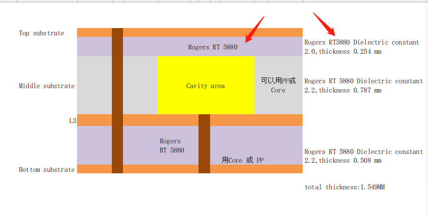
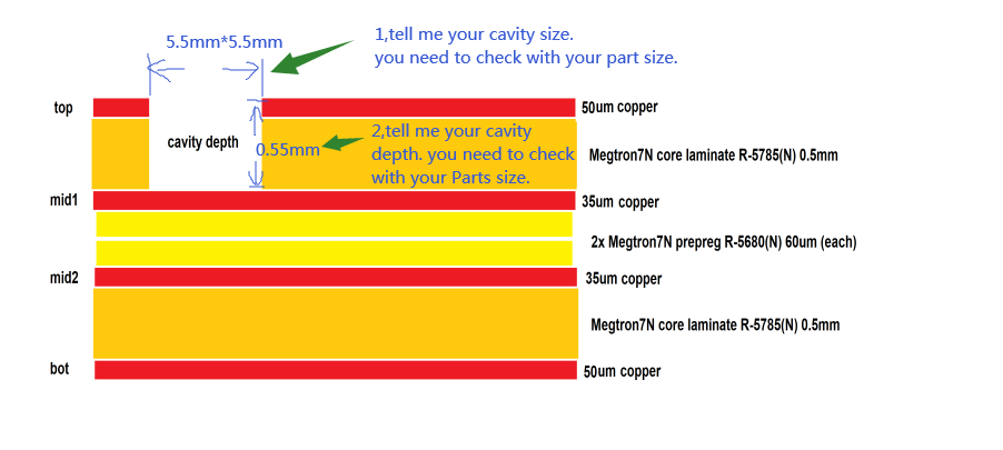
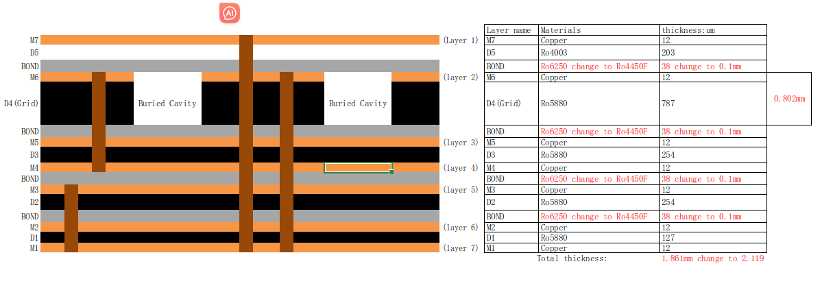
Buried type Cavity PCB
What is the Cavity PCB Fabrication Process?
The fabrication process for a cavity PCB involves several steps, including substrate preparation, cavity formation, circuit patterning, component assembly, and testing. Here’s a general overview of the process:
- Substrate Selection: Choose a suitable substrate material based on the application requirements, considering factors such as thermal conductivity, dielectric properties, and mechanical strength. Common substrate materials include FR4, metal-core PCBs, and ceramic substrates.
- Cavity Formation: Use mechanical milling, routing, or drilling techniques to create cavities within the substrate according to the design specifications. CNC (Computer Numerical Control) machines are often used for precision cavity milling. The cavities may be single-sided, double-sided, or multilayered, depending on the complexity of the design.
- Surface Preparation: Clean the substrate surface thoroughly to remove any contaminants or residues that could affect the adhesion of copper and other materials during subsequent processing steps.
- Circuit Patterning: Apply a layer of copper foil to the substrate surface through processes such as lamination or electrodeposition. Use photolithography and etching techniques to create circuit patterns on the copper layer, defining the conductive traces, pads, and vias according to the PCB design.
- Plating and Surface Finish: Plate the circuitry with additional layers of copper to enhance conductivity and facilitate solderability. Apply surface finishes such as HASL (Hot Air Solder Leveling), ENIG (Electroless Nickel Immersion Gold), or OSP (Organic Solderability Preservative) to protect the exposed copper surfaces from oxidation and ensure reliable solder joints.
- Component Assembly: Mount electronic components onto the PCB surface or within the cavities using automated pick-and-place machines or manual soldering techniques. Ensure proper alignment and soldering of components to the circuitry, taking into account any spatial constraints imposed by the cavity design.
- Encapsulation and Sealing: Optionally, encapsulate the cavity PCB assembly with protective coatings or encapsulant materials to enhance durability, moisture resistance, and mechanical stability. Seal any openings or interfaces to prevent ingress of contaminants and ensure the integrity of the enclosure.
- Testing and Inspection: Conduct electrical testing, functional testing, and inspection of the finished cavity PCB assembly to verify conformance to design specifications and quality standards. Perform checks for continuity, shorts, insulation resistance, and other parameters using automated test equipment and visual inspection techniques.
- Packaging and Shipping: Package the cavity PCB assemblies securely for protection during transportation and storage. Label the packages with relevant information such as part numbers, revision codes, and handling instructions before shipping to customers or assembly facilities.
By following these fabrication steps with precision and attention to detail, manufacturers can produce high-quality cavity PCBs that meet the performance, reliability, and regulatory requirements of their intended applications.
Buried type Cavity PCB
How do you manufacture a Cavity PCB?
Manufacturing a cavity PCB involves a series of steps that are similar to traditional PCB fabrication processes, with additional considerations for creating the cavity within the board. Here’s a step-by-step guide to manufacturing a cavity PCB:
- Design Preparation: Begin with the PCB design phase, where the cavity structure is integrated into the board layout using PCB design software. Ensure that the design meets the specific requirements of the application, including component placement, signal integrity, thermal management, and EMI shielding.
- Material Selection: Choose the appropriate substrate material based on the application requirements and the desired properties of the cavity PCB, such as thermal conductivity, dielectric constant, and mechanical strength. Common substrate materials include FR4, metal-core PCBs (MCPCB), and ceramic substrates.
- Cavity Formation: Use specialized CNC (Computer Numerical Control) milling or routing machines to create the cavity within the PCB substrate according to the design specifications. The cavity can be milled from one or both sides of the board, depending on the complexity of the design and the desired depth of the cavity.
- Surface Preparation: Clean the substrate surface thoroughly to remove any contaminants or residues that could affect the adhesion of copper and other materials during subsequent processing steps. Surface cleaning can be done using chemical cleaning agents, mechanical scrubbing, or plasma treatment.
- Circuit Patterning: Apply a layer of copper foil to the substrate surface through processes such as lamination or electrodeposition. Use photolithography and etching techniques to create circuit patterns on the copper layer, defining the conductive traces, pads, and vias according to the PCB design.
- Plating and Surface Finish: Plate the circuitry with additional layers of copper to enhance conductivity and facilitate solderability. Apply surface finishes such as HASL (Hot Air Solder Leveling), ENIG (Electroless Nickel Immersion Gold), or OSP (Organic Solderability Preservative) to protect the exposed copper surfaces from oxidation and ensure reliable solder joints.
- Component Assembly: Mount electronic components onto the PCB surface or within the cavities using automated pick-and-place machines or manual soldering techniques. Ensure proper alignment and soldering of components to the circuitry, taking into account any spatial constraints imposed by the cavity design.
- Encapsulation and Sealing: Optionally, encapsulate the cavity PCB assembly with protective coatings or encapsulant materials to enhance durability, moisture resistance, and mechanical stability. Seal any openings or interfaces to prevent ingress of contaminants and ensure the integrity of the enclosure.
- Testing and Inspection: Conduct electrical testing, functional testing, and inspection of the finished cavity PCB assembly to verify conformance to design specifications and quality standards. Perform checks for continuity, shorts, insulation resistance, and other parameters using automated test equipment and visual inspection techniques.
- Packaging and Shipping: Package the cavity PCB assemblies securely for protection during transportation and storage. Label the packages with relevant information such as part numbers, revision codes, and handling instructions before shipping to customers or assembly facilities.
By following these manufacturing steps with precision and attention to detail, manufacturers can produce high-quality cavity PCBs that meet the performance, reliability, and regulatory requirements of their intended applications.
How much should a Cavity PCB cost?
The cost of a cavity PCB can vary significantly depending on various factors such as the complexity of the design, the type of substrate material used, the number of layers, the quantity ordered, and the manufacturing processes involved. Here are some factors that can influence the cost:
- Design Complexity: Intricate cavity designs with multiple layers, dense component placement, and high-speed signal requirements may incur higher manufacturing costs due to the increased complexity of fabrication and assembly.
- Substrate Material: The choice of substrate material can affect the cost of the PCB. Specialty materials such as metal-core PCBs or ceramic substrates may be more expensive than standard FR4 substrates due to their unique properties and manufacturing processes.
- Cavity Depth and Dimensions: Larger and deeper cavities may require specialized milling or routing equipment, which can contribute to higher manufacturing costs.
- Surface Finish and Plating: Different surface finishes and plating options have varying costs. For example, gold plating is more expensive than HASL (Hot Air Solder Leveling) or OSP (Organic Solderability Preservative) finishes.
- Quantity Ordered: Economies of scale apply to PCB manufacturing, meaning that larger order quantities typically result in lower per-unit costs. However, prototyping or low-volume production runs may incur higher costs per unit.
- Manufacturing Technology: Advanced manufacturing techniques such as laser drilling, HDI (High-Density Interconnect), and sequential lamination can increase the cost but may be necessary for specific design requirements.
- Additional Services: Extra services such as testing, inspection, conformal coating, and component sourcing may add to the overall cost of the cavity PCB.
It’s challenging to provide an exact cost without specific details about the PCB design and manufacturing requirements. Generally, it’s advisable to consult with PCB manufacturers and provide them with detailed specifications to obtain accurate price quotes for cavity PCB fabrication. Additionally, obtaining multiple quotes from different manufacturers can help in comparing costs and selecting the most cost-effective option.
What is Cavity PCB base material?
The base material used for cavity PCBs can vary depending on the specific requirements of the application and the desired properties of the PCB. Some common base materials used for cavity PCBs include:
- FR-4: FR-4 (Flame Retardant 4) is a widely used standard substrate material for PCBs due to its affordability, availability, and good overall performance. It consists of layers of woven fiberglass cloth impregnated with an epoxy resin binder. FR-4 is suitable for many applications but may not offer the highest thermal conductivity or mechanical strength compared to other materials.
- Metal-Core PCBs (MCPCB): Metal-core PCBs feature a metal core, typically aluminum or copper, sandwiched between layers of dielectric material (usually FR-4 or a thermally conductive material). The metal core provides excellent thermal conductivity, making MCPCBs ideal for applications requiring efficient heat dissipation, such as high-power LEDs and power electronics.
- Ceramic Substrates: Ceramic substrates offer superior thermal conductivity, mechanical strength, and stability compared to organic substrates like FR-4. Common ceramic materials used for PCB substrates include aluminum oxide (Al2O3) and aluminum nitride (AlN). Ceramic substrates are suitable for high-frequency, high-power, and high-temperature applications, but they are typically more expensive and less flexible than organic substrates.
- Thermally Conductive Materials: Some cavity PCBs may utilize specialized thermally conductive materials, such as metal-filled polymer composites or thermally conductive plastics, as the base material. These materials offer enhanced thermal management capabilities while maintaining flexibility and cost-effectiveness.
The choice of base material for a cavity PCB depends on factors such as thermal management requirements, mechanical stability, dielectric properties, cost considerations, and compatibility with manufacturing processes. Designers should carefully evaluate these factors to select the most suitable base material for their specific application.
Which company makes Cavity PCB?
Many companies can manufacture cavity PCBs, including some well-known PCB manufacturers and electronic component suppliers. Some of these companies specialize in providing customized cavity PCB design and manufacturing services to meet specific application requirements.
Some well-known PCB manufacturers and electronic component suppliers include Foxconn, Oupai Electronics, Jiangsu Lian Electronics Technology, Xilinx Electronics, and GoerTek. These companies have advanced production equipment, rich experience, and professional teams capable of providing customers with high-quality cavity PCB products and solutions.
As for our company, we can also produce cavity PCBs. As a professional electronic manufacturing service provider, we have advanced production equipment and technology, as well as an experienced engineering team. We can provide customized cavity PCB design and manufacturing services according to customer requirements, including:
- Engineering Design Support: Our engineering team can collaborate with customers to provide design support for cavity PCBs, including technical consultation on wiring, heat dissipation design, EMI/EMC analysis, and more.
- Manufacturing Capability: We have advanced PCB production lines and processes that can produce various types of cavity PCBs, including single-sided, double-sided, and multilayer structures, as well as different types of substrate materials.
- Quality Assurance: We strictly adhere to international quality management system standards to ensure stable and reliable product quality. Our production process undergoes rigorous quality control and inspection to meet customer requirements and standards.
- Delivery Lead Time: We have efficient production capacity and supply chain management systems to deliver customer orders promptly, ensuring smooth progress of customer projects.
In conclusion, our company has the technical strength, production capacity, and professional team to produce cavity PCBs, providing customers with high-quality, customized solutions. If you are interested in our services, please feel free to contact us, and we will be happy to provide support and service.
What are the 7 qualities of good customer service?
Good customer service is essential for maintaining customer satisfaction and loyalty. Here are seven qualities that characterize good customer service:
- Empathy: Good customer service representatives demonstrate empathy by understanding and relating to the customer’s feelings, concerns, and needs. They listen actively, show compassion, and strive to put themselves in the customer’s shoes to provide appropriate support and assistance.
- Responsiveness: Good customer service is prompt and responsive. Representatives acknowledge customer inquiries, requests, and issues in a timely manner, ensuring that customers feel valued and their concerns are addressed promptly.
- Professionalism: Good customer service is conducted with professionalism and courtesy. Representatives maintain a positive attitude, use clear and respectful communication, and conduct themselves in a manner that reflects positively on the company.
- Knowledgeability: Good customer service representatives possess the knowledge and expertise necessary to answer customer questions, resolve issues, and provide helpful guidance and advice. They stay informed about the company’s products, services, policies, and procedures to provide accurate information to customers.
- Flexibility: Good customer service involves being adaptable and flexible to meet the diverse needs and preferences of customers. Representatives are willing to accommodate customer requests, offer customized solutions, and adjust their approach as needed to ensure customer satisfaction.
- Problem-solving skills: Good customer service representatives are effective problem solvers. They approach customer issues with a positive attitude, analyze the situation thoroughly, identify root causes, and work proactively to find solutions that meet the customer’s needs and expectations.
- Consistency: Good customer service is consistent across all interactions and touchpoints. Customers expect a consistent level of service quality regardless of whether they interact with the company in person, over the phone, via email, or through other channels. Consistency builds trust and reinforces the company’s reputation for excellence in customer service.
By embodying these qualities, companies can deliver exceptional customer service experiences that foster loyalty, positive word-of-mouth referrals, and long-term relationships with customers.
FAQs
What is a cavity PCB?
A cavity PCB, or cavity printed circuit board, is a type of PCB design where one or more sections of the board are recessed or “cavities” are created within the board itself. These cavities can serve various purposes such as housing components, providing shielding, or reducing electromagnetic interference (EMI).
What are the advantages of using a cavity PCB?
Cavity PCBs offer several advantages, including compactness, improved thermal management, enhanced EMI shielding, and protection of sensitive components from external influences. By integrating components into the board itself, rather than placing them on the surface, engineers can create more efficient and reliable electronic devices.
What types of applications are cavity PCBs used for?
Cavity PCBs are used in a wide range of applications across industries such as telecommunications, aerospace, automotive, medical devices, and consumer electronics. They are particularly well-suited for applications requiring compactness, high reliability, and effective thermal management.
How are cavity PCBs manufactured?
The manufacturing process for cavity PCBs involves several steps, including substrate preparation, cavity formation, circuit patterning, component assembly, and testing. Specialized CNC milling or routing machines are used to create the cavities within the PCB substrate, followed by conventional PCB fabrication processes.
What considerations should be taken into account when designing a cavity PCB?
When designing a cavity PCB, engineers should consider factors such as component placement, cavity dimensions, material selection, EMI shielding, thermal management, manufacturability, and environmental considerations. Careful planning and adherence to design guidelines are essential to ensure successful implementation.
Are there any limitations or challenges associated with cavity PCBs?
While cavity PCBs offer many benefits, they also present certain challenges such as increased complexity, higher manufacturing costs, and potential difficulties with assembly and testing. Designers should carefully evaluate these factors and weigh them against the desired benefits when deciding whether to use cavity PCBs for a particular application.
Where can I find a manufacturer for cavity PCBs?
Many PCB manufacturers offer cavity PCB fabrication services. It’s advisable to research and contact several manufacturers to compare capabilities, pricing, and lead times. Additionally, working with a manufacturer that specializes in advanced PCB technologies and has experience with cavity PCBs can help ensure a successful outcome.