
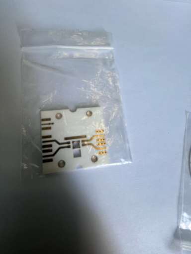
What is Ceramic Packaging Substrate?
We are a professional Ceramic packaging substrate supplier, we mainly produce ultra-small bump pitch Ceramic PCBs and Ceramic bga package substrate from 1layer to 30 layers, ultra-small trace and spacing with 9um/9um.
Ceramic packaging substrates are integral in the realm of electronic components, particularly within the semiconductor domain. Fashioned from materials such as aluminum oxide (alumina) or aluminum nitride, these substrates serve as a steadfast and reliable groundwork for the installation and interconnection of semiconductor chips.
Within the realm of electronic devices, ceramic packaging substrates fulfill a spectrum of functions:
Efficient Heat Management: Harnessing their commendable thermal conductivity, ceramics proficiently disperse heat, mitigating the risk of semiconductor devices reaching excessive temperatures.
Robust Mechanical Support: The substrate furnishes a resilient framework that buttresses semiconductor chips, shielding delicate electronic components from mechanical strains and environmental exigencies.
Superlative Electrical Insulation: Ceramic materials function as impeccable insulators, preempting unwarranted electrical interactions among diverse components residing on the substrate.
Facilitation of Signal Transmission: The substrate streamlines the transmission of electrical signals across various segments of the electronic device, oftentimes incorporating conductive traces and vias for this purpose.
Seamless Hermetic Sealing: In specific scenarios, ceramic packaging substrates are enlisted to establish a hermetic seal, fortifying enclosed electronic components against moisture and sundry environmental variables.
Widely deployed in sectors necessitating top-tier reliability, thermal prowess, and electrical insulation, ceramic packaging substrates find recurrent application in power modules, integrated circuits, and assorted semiconductor devices. Their pivotal role in sustaining unwavering electrical and thermal attributes is imperative for ensuring optimal functionality and protracted endurance.
Ceramic PCBs
What is the function of Ceramic Packaging Substrate?
Enter the ceramic packaging substrate, a true maestro in the symphony of electronic components. This versatile player wears multiple hats, each contributing to the seamless performance of semiconductor devices:
Thermal Choreographer: Picture ceramics like alumina or aluminum nitride taking center stage, gracefully conducting heat away from semiconductor devices. The substrate’s choreography ensures a temperature-balanced performance, preventing any overheating drama.
Structural Guardian: Acting as a dependable guardian, the substrate provides a robust framework—like a silent sentinel—cradling semiconductor chips and shielding them from the tumultuous world of mechanical stresses and vibrations.
Electrical Diplomat: Ceramic materials step into the role of diplomatic peacemakers. The substrate acts as a mediator, preventing electrical skirmishes between different components and maintaining a harmonious coexistence in the electronic realm.
Signal Maestro: Armed with conductive traces and vias, the substrate transforms into a maestro orchestrating the intricate dance of electrical signals. It conducts this symphony, ensuring that every component is in tune and in communication.
Hermetic Protector: In certain scenes, our ceramic protagonist dons the cloak of a hermetic protector. Sealing components with an airtight embrace, it shields them from moisture, contaminants, and environmental mischief, ensuring a long and reliable performance.
In essence, the ceramic packaging substrate is the behind-the-scenes virtuoso, managing the heat, providing a sturdy support system, orchestrating electrical harmony, directing the signal ballet, and standing guard against environmental adversaries—all for the flawless execution of the electronic masterpiece.
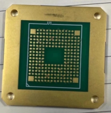
Ceramic Packaging Substrate
What are the different types of Ceramic Packaging Substrate?
In the expansive universe of electronic applications, a diverse lineup of ceramic packaging substrates steps forward, each boasting distinctive traits tailored to specific demands. The art of selecting among these substrates involves a meticulous dance, considering factors such as thermal conductivity, cost dynamics, and the intricate needs of the application. Let’s explore the cast:
Alumina (Aluminum Oxide): A perennial star, alumina takes a prominent role as a versatile player in packaging substrates. With its remarkable thermal conductivity, electrical insulation prowess, and mechanical resilience, alumina substrates navigate through various electronic scenarios with finesse.
Aluminum Nitride (AlN): Making a notable entrance with stellar thermal conductivity, aluminum nitride assumes a pivotal role in applications where efficient heat dissipation is crucial—especially in the dynamic realm of power electronics. AlN substrates also exhibit commendable electrical insulation properties.
Silicon Nitride (Si3N4): Stepping onto the stage with exceptional thermal shock resistance and unwavering reliability, silicon nitride is finely tuned for high-temperature environments. Si3N4 substrates play a crucial role in meeting specific packaging requirements for semiconductors.
Beryllium Oxide (BeO): Unveiling unmatched thermal conductivity, beryllium oxide takes center stage where seamless heat transfer is non-negotiable. However, a note of caution accompanies its performance—the toxicity of beryllium restricts its usage in certain regions.
Zirconia (ZrO2): While not claiming the spotlight as frequently as alumina or aluminum nitride, zirconia ceramics bring a unique combination of high strength and toughness to the stage. They carve a niche in applications calling for these distinctive properties.
Ferrites: Injecting a magnetic twist into the narrative, ferrite ceramic materials command attention when magnetic properties become the focal point—especially in the crafting of specific inductors.
The process of substrate selection, masterfully directed by engineers, intricately weaves together the elements of thermal performance, electrical characteristics, mechanical resilience, and cost-effectiveness. It’s a symphony thoughtfully composed to meet the nuanced needs of electronic devices and semiconductor applications, ensuring a harmonious performance on the grand stage of technology.
What is the relationship between Ceramic Packaging Substrate and IC packaging?
In the intricate narrative of semiconductor technology, ceramic packaging substrates and IC (Integrated Circuit) packaging take on dynamic roles, engaging in a collaborative performance akin to a well-coordinated play. Let’s delve into the evolving script of this synergy:
Foundational Anchoring:
Ceramic Packaging Substrate: It assumes a pivotal role as the anchor, providing a steadfast foundation for the mounting of semiconductor chips—a crucial act in the unfolding drama of IC packaging.
IC Packaging: Beyond a mere supporting act, the ceramic substrate becomes the stage where semiconductor dies find their place, embodying a central role in the unfolding narrative of IC packaging.
Thermal Choreography:
Ceramic Packaging Substrate: Applauded for its thermal prowess, the ceramic substrate takes the lead in choreographing the elegant dissipation of heat generated by semiconductor devices.
IC Packaging: Within the intricate dance of IC packages, the nuanced management of heat becomes a spotlight moment. The ceramic substrate conducts this thermal symphony, ensuring a performance where temperature dynamics gracefully unfold.
Electrical Sonata:
Ceramic Packaging Substrate: With its adept electrical insulation capabilities, the ceramic substrate conducts a harmonious sonata, preventing discordant electrical interactions among diverse components.
IC Packaging: Electrical insulation transcends a mere background theme; it becomes a vital melody in IC packaging. The ceramic substrate’s insulating finesse contributes to the symphonic electrical integrity of the packaged IC.
Signal Ballet:
Ceramic Packaging Substrate: Unveiling an intricately choreographed arrangement of conductive traces and vias, the substrate facilitates the graceful ballet of electrical signals between different segments.
IC Packaging: Signal transmission evolves into a ballet of precision. The design on the ceramic substrate directs this intricate dance, ensuring a seamless flow of communication among the various components housed within the IC.
Guardian of Components:
Ceramic Packaging Substrate: At critical junctures, the ceramic substrate transforms into a vigilant guardian, crafting a hermetic seal that shields semiconductor components from the environmental elements.
IC Packaging: Protection and encapsulation emerge as pivotal acts in the unfolding narrative of IC packaging. The ceramic substrate becomes the guardian, ensuring the encapsulated IC components endure and perform reliably.
In essence, the collaborative narrative between ceramic packaging substrates and IC packaging is an evolving symphony, where each partner brings its unique notes to compose a seamless and reliable masterpiece in the captivating storyline of semiconductor technology. It’s a play where the ceramic substrate gracefully adapts to diverse roles, ensuring a stellar performance on the semiconductor stage.
How does Ceramic Packaging Substrate differ from traditional PCB?
Ceramic packaging substrates and traditional PCBs (Printed Circuit Boards) are essential players in the orchestration of electronic devices, marked by their unique material compositions, thermal dynamics, and application landscapes. Let’s unravel the contrasting facets:
Material Composition Ballet:
Ceramic Packaging Substrate: Forged from an array of ceramics including alumina, aluminum nitride, silicon nitride, beryllium oxide, and zirconia, these substrates seamlessly marry the virtues of elevated thermal conductivity and outstanding electrical insulation.
Traditional PCB: Constructed from materials like fiberglass-reinforced epoxy or other composite blends, the traditional PCB unveils a stratified structure, where copper traces engage in a coordinated choreography, crafting a rhythmic dance that brings the circuit to life.
Thermal Choreography:
Ceramic Packaging Substrate: Celebrated for its leading role in the thermal arena, ceramic substrates take charge in applications where the elegant dissipation of heat is non-negotiable, especially in high-power electronic devices.
Traditional PCB: Exhibiting thermal moves of a different cadence, it generally showcases lower thermal conductivity, potentially limiting its performance in high-temperature environments.
Electrical Harmony Sonata:
Ceramic Packaging Substrate: Strikes a chord with excellent electrical insulation, conducting a symphony that prevents discordant electrical interactions and short circuits between components.
Traditional PCB: Presents its own electrical melody, offering insulation while acknowledging that its notes may not reach the same heights as those produced by ceramics.
Mechanical Strength Ballet:
Ceramic Packaging Substrate: Takes center stage with a display of high mechanical strength and durability, fitting seamlessly into roles demanding robustness.
Traditional PCB: While boasting stability, it might not execute the same strength choreography as ceramics.
Applications Symphony:
Ceramic Packaging Substrate: Commands attention in applications that demand top-tier thermal performance, reliability, and resilience in challenging environments—often gracing the semiconductor packaging arena.
Traditional PCB: Demonstrates versatility in a diverse ensemble of electronic devices, from the familiar hum of consumer electronics to the industrial crescendo.
Cost Overture:
Ceramic Packaging Substrate: Takes a bow with a higher price tag, reflecting the investment in ceramic materials and specialized manufacturing processes.
Traditional PCB: Strikes a more economical note, often becoming the preferred choice for a wide range of applications.
Specific Use Scenarios Drama:
Ceramic Packaging Substrate: Assumes a leading role in high-performance electronic devices, power modules, and scenarios where thermal management takes center stage.
Traditional PCB: Plays a versatile character, stepping into various electronic devices and confidently embracing roles across the technological spectrum.
In essence, the interplay between ceramic packaging substrates and traditional PCBs forms a symphony, with each component contributing its unique notes to the electronic composition. The choice between them becomes a decision nuanced by the specific needs of the electronic device, allowing ceramics to shine in high-performance and thermal management acts while traditional PCBs play their versatile tune in a myriad of applications.
What is the main structure and production technology of Ceramic Packaging Substrate?
Crafting a Ceramic Packaging Substrate involves a meticulous dance of materials and processes. Let’s unravel the intricate steps that shape its main structure and production technology:
Main Structure:
Canvas of Ceramics:
Base Material: Choose from a palette of ceramic compositions—alumina, aluminum nitride, silicon nitride, beryllium oxide, zirconia, each bringing its unique notes to the substrate’s performance.
Layers in Harmony:
Conductive Traces and Vias: Paint the ceramic canvas with conductive traces and vias, creating a symphony of electrical connectivity.
Dielectric Layers: Introduce layers that act as insulating melodies, preventing any short circuits and ensuring a harmonious composition.
Metal Layers: Sometimes, add extra metal layers for specific features, creating subtle nuances in the substrate’s performance.
Surface Finale:
Metallization Magic: Apply metallization to selected areas, adding a touch of brilliance for improved solderability and bonding during the assembly act.
Production Artistry:
Substrate Sculpting:
Powder Alchemy: Begin with the preparation of ceramic powders, selecting and blending them to achieve the desired properties.
Forming Elegance: Shape the ceramic powder into a green body, employing techniques like dry pressing or tape casting to sculpt the initial form.
Sintering Symphony:
High-Temperature Ballet: Take the green body through a high-temperature sintering process, where the ceramic particles fuse and dance into a dense, solid substrate.
Densification Drama: Witness the transformation as densification enhances mechanical and thermal qualities, giving the substrate a strong and resilient character.
Surface Poetry:
Etching Artistry: Employ photolithography and etching to carve out the patterns of conductive traces and vias, creating an artistic expression on the ceramic canvas.
Metallization Alchemy: Introduce metal layers with deposition techniques, adding a metallic flourish to specific areas for enhanced conductivity.
Surface Finish Serenade:
Plating or Coating Elegance: Elevate the substrate’s appearance with plating or coating, offering a refined surface finish that complements subsequent assembly steps.
Quality Ballad:
Testing Symphony: Perform various tests—a thermal conductivity overture, electrical testing sonata, and visual inspection chorale—to ensure the substrate hits the right notes in quality.
Component Ballet:
Die Attach and Wire Bonding Pas de Deux: Embark on the assembly act, where semiconductor components are delicately attached using die attach materials, and wire bonding connects them to the conductive traces.
Encapsulation Crescendo (Optional):
Hermetic Sealing Finale: In certain scenes, encapsulate the substrate, providing a protective layer against environmental elements, creating a climactic finish.
Final Testing Curtain Call:
Functional Testing Overture: Conclude the production with a grand finale of functional testing, ensuring the substrate performs flawlessly in its electronic role.
The production technology of Ceramic Packaging Substrates is an artful composition, blending materials and processes to create a masterpiece worthy of the electronic symphony.
Frequently Asked Questions (FAQs)
How does a Ceramic Packaging Substrate differ from a traditional PCB?
The distinction lies in material composition. Ceramic Packaging Substrates, with their high thermal conductivity, differ from traditional PCBs made of materials like fiberglass-reinforced epoxy. Ceramics excel in high-heat and high-performance scenarios.
What does the production process of Ceramic Packaging Substrates entail?
Production involves steps such as powder preparation, forming (utilizing techniques like dry pressing or tape casting), sintering (a high-temperature fusion of ceramic particles), surface preparation (including etching and metallization), and assembly (featuring die attach and wire bonding). Rigorous quality control tests guarantee adherence to specifications.
Can Ceramic Packaging Substrates be utilized for hermetic sealing?
Yes, in specific applications, Ceramic Packaging Substrates can be employed for hermetic sealing. This involves creating a secure, impermeable seal to shield semiconductor components from environmental elements like moisture.
What testing procedures are conducted during the production of Ceramic Packaging Substrates?
Testing encompasses thermal conductivity assessments, electrical testing, and visual inspections. These tests guarantee that the substrate meets rigorous quality standards and performs reliably in electronic devices.
Is the cost of Ceramic Packaging Substrates higher compared to traditional PCBs?
Yes, generally, the cost of Ceramic Packaging Substrates is higher than that of traditional PCBs. This cost difference is attributed to the specialized materials and manufacturing processes involved in crafting ceramic substrates.
Conclusion
In summary, Ceramic Packaging Substrates emerge as pivotal players in the electronic orchestration, offering a harmonious blend of thermal efficiency, electrical insulation, and mechanical robustness. Their role as a foundational platform for semiconductor chips and their adept management of thermal dynamics position them at the forefront of high-performance applications.
The production narrative of Ceramic Packaging Substrates unfolds like a carefully choreographed ballet, with each step—from powder preparation to assembly—contributing to the creation of a resilient substrate. The palette of ceramic materials adds a layer of versatility, allowing customization to meet the unique demands of diverse applications.
As they take the stage, Ceramic Packaging Substrates become protagonists in high-performance electronic devices, power modules, and environments where thermal equilibrium is paramount. Their reliability in challenging conditions solidifies their place in semiconductor packaging, where they become guardians of electronic precision.
While the cost of Ceramic Packaging Substrates may carry a premium compared to traditional PCBs, it becomes a justified investment in the symphony of specialized properties and manufacturing finesse they bring to electronic assemblies.
In essence, Ceramic Packaging Substrates compose a symphony of support in the electronic ensemble, ensuring a robust foundation for the integration and seamless operation of semiconductor devices. As technological landscapes evolve, the ongoing refinement of Ceramic Packaging Substrates promises not just reliability but a continuing crescendo of innovation in the electronic realm.