
We are a professional Ceramic substrate supplier, we mainly produce ultra-small bump pitch substrate, ultra-small trace and spacing packaging substrate and PCBs.
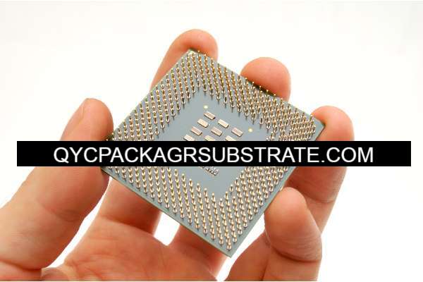
In the realm of modern electronics, ceramic packaging substrates stand as essential elements, providing a specialized material to establish a stable and dependable base for the installation of integrated circuits (ICs) and diverse electronic components. Constructed primarily from ceramics such as alumina or aluminum nitride, these substrates undergo engineering to precisely cater to the unique requirements of electronic elements.
Key to their functionality is the notable thermal conductivity of ceramic packaging substrates, efficiently dissipating heat generated during the operation of electronic devices. This property is especially crucial in applications where high temperatures might negatively impact performance.
Another significant attribute is the admirable electrical insulation provided by these substrates. This insulation safeguards electronic components from undesired interactions, ensuring the stability of electrical signals within circuits and preventing issues such as short circuits, contributing substantially to overall system reliability.
Manufacturing processes involve diverse techniques like thick film printing, deposition, and other processes that shape substrates into various forms and sizes. This adaptability in manufacturing allows for customization, catering to the specific needs of different electronic applications.
Widely utilized in crucial electronic components such as microprocessors, radio frequency modules, and power amplifiers, ceramic packaging substrates are indispensable in environments where reliability and stability are paramount. Their capacity to endure high temperatures, frequencies, and power demands underscores their importance in cutting-edge electronic devices.
In summary, ceramic packaging substrates, characterized by their specialized composition and tailored features, play a foundational role in ensuring the reliability and stability of electronic components. As technology advances, these substrates continue to be crucial in facilitating the seamless operation of intricate circuits that power our modern world.
How Does Ceramic Packaging Substrate Function?
The essential role of ceramic packaging substrates in modern electronics centers around establishing a conducive environment for electronic components. Specifically engineered with materials like alumina or aluminum nitride, these substrates cater to the unique demands of electronic elements. A critical aspect of their functionality lies in efficient thermal management.
As electronic components, particularly ICs, generate heat during operation, ceramic packaging substrates act as pathways for the effective transfer of this heat away from the components. This prevents overheating, a condition that can lead to performance degradation and potential damage. The controlled thermal environment provided by ceramic substrates helps maintain components within optimal operating temperatures, preserving circuit integrity and ensuring consistent functionality.
Beyond thermal management, ceramic packaging substrates offer electrical insulation, safeguarding electronic components from undesired interactions and ensuring the stability of electrical signals within circuits. This dual functionality positions ceramic packaging substrates as key contributors to the reliable operation and longevity of electronic devices.
In essence, ceramic packaging substrates are instrumental in crafting an environment conducive to electronic components, emphasizing effective thermal management. Their ability to dissipate heat and offer electrical insulation significantly contributes to the overall reliability and sustained performance of electronic devices over time.
What Types of Ceramic Packaging Substrate Exist?
Ceramic packaging substrates take a pivotal role in the dynamic realm of technology, offering three distinct types thoughtfully designed to meet diverse application requirements. These substrates—multi-layer ceramic substrates (MLCs), low-temperature co-fired ceramics (LTCCs), and high-temperature co-fired ceramics (HTCCs)—represent an amalgamation of material science, precise engineering, and technological innovation.
Starting with multi-layer ceramic substrates (MLCs), these exemplify sophistication in electronic packaging. Their layered composition, featuring multiple ceramic layers, facilitates high-density circuitry, allowing for the precise integration of conductive pathways to enable efficient electrical signal transmission. MLCs are indispensable in applications demanding intricate circuit designs, notably in advanced semiconductor packaging and microelectronics.
In essence, the trio of MLCs, LTCCs, and HTCCs presents a comprehensive palette of ceramic substrates, each uniquely suited to specific technological needs. MLCs thrive in intricate circuitry, forming the backbone of advanced semiconductor packaging. LTCCs offer thermal resilience and the integration of passive components, playing a pivotal role in miniaturized electronic systems. Meanwhile, HTCCs stand as pillars of strength, ensuring reliability in the face of extreme environmental challenges.
As we navigate the ever-evolving technology landscape, these ceramic substrates become unsung heroes, providing a solid foundation for the electronic innovations of tomorrow. The relentless pursuit of innovation continues, and MLCs, LTCCs, and HTCCs stand poised to support the next wave of technological advancements, ushering in possibilities across diverse industries.
How Does Ceramic Packaging Substrate Differ from PCBs?
The ability of ceramics to adeptly transfer and dissipate heat becomes paramount in scenarios where electronic components are densely packed, as often encountered in the intricate layouts of SLPs. This heightened thermal performance significantly contributes to the improved overall system reliability demanded by cutting-edge electronic devices.
In the domain of high-density interconnect (HDI) substrates, ceramic packaging substrates reclaim the spotlight. HDI substrates, prized for their compact designs and demand for high signal integrity, find an optimal ally in ceramic substrates. The superior thermal conductivity and electrical insulation properties of ceramics play a dual role here. Efficient heat dissipation ensures stable operating temperatures, shielding intricate electronic components, while the insulation properties safeguard against unwanted interactions, ensuring the consistent and uninterrupted flow of electrical signals in densely populated circuits.
The strategic use of ceramics is not just a choice; it is a precision-engineered solution that positions ceramic packaging substrates not as mere alternatives but as indispensable components in applications demanding advanced thermal management. The meticulous consideration for material selection and manufacturing processes underscores the irreplaceable role of ceramic substrates in the dynamic landscape of contemporary electronics.
In summation, the odyssey through the realm of ceramic packaging substrates illuminates their distinct attributes and underscores their pivotal role in guaranteeing the reliability, longevity, and optimal performance of electronic devices. As technological frontiers expand, ceramic packaging substrates stand resilient as foundational elements, contributing profoundly to the flawless operation of intricate circuits that power our interconnected world.
What Comprises the Main Structure and Production Technologies of Ceramic Packaging Substrate?
The intricate structure of ceramic packaging substrates is designed to serve as a reliable foundation for mounting integrated circuits (ICs) and various electronic components. A closer examination reveals distinct layers with specific functions, and advancements in production technologies, notably High-Density Interconnect (HDI) fabrication and semi-additive methods, significantly contribute to enhancing precision and efficiency in ceramic packaging substrate manufacturing.
Structure of Ceramic Packaging Substrate:
Conductor Layers:
Above the base layer, multiple conductor layers, typically made of materials like copper or gold, facilitate the flow of electrical signals between different components.
Dielectric Layers:
Interposed between the conductor layers, dielectric layers prevent electrical interference or short circuits, maintaining separation between adjacent conductive traces.
Via Structures:
Vertical connections between layers are established through via structures, small holes filled with conductive material to enable the transfer of electrical signals.
Surface Finish:
The topmost layer serves as the surface finish, protecting the substrate and allowing for the attachment of electronic components using materials like solder mask.
Production Technologies:
HDI Fabrication Techniques:
Semi-Additive Methods:
Semi-additive methods focus on selective material deposition, optimizing resource usage and enhancing precision. This approach is instrumental in creating intricate patterns and features on the substrate.
Thick Film Printing:
Thick film printing involves depositing a thick paste with conductive or resistive materials onto the substrate surface, followed by firing to create conductive paths or resistors.
In summary, the complex structure of ceramic packaging substrates, comprising distinct layers with specific functions, forms a robust foundation for electronic components. Innovations in production technologies, particularly HDI fabrication and semi-additive methods, drive efficiency and precision in manufacturing, contributing to the evolution of these critical components in the ever-advancing realm of electronics.
Frequently Asked Questions (FAQs) About Ceramic Packaging Substrate
Can you elaborate on semi-additive methods and their role in ceramic packaging substrate manufacturing?
Semi-additive methods in ceramic packaging substrate manufacturing involve the selective deposition of material only where it is needed. This approach minimizes waste and enhances precision by adding material in specific areas, optimizing resource usage. Semi-additive methods play a crucial role in creating intricate patterns and fine features on ceramic substrates, contributing to more efficient production processes.
What are High-Density Interconnect (HDI) fabrication techniques, and how do they enhance ceramic packaging substrate production?
HDI fabrication techniques involve advanced manufacturing processes aimed at achieving higher routing densities, finer traces, and smaller vias in ceramic packaging substrates. These techniques include laser drilling and sequential build-up processes, allowing for the creation of intricate structures with reduced size. The use of HDI techniques contributes to the overall precision and efficiency of ceramic packaging substrate production, aligning with the demand for smaller and more advanced electronic devices.
What are semi-additive methods, and how do they impact ceramic packaging substrate manufacturing?
Semi-additive methods involve the selective deposition of material only where it is needed, minimizing waste and enhancing precision. In ceramic packaging substrate manufacturing, these methods contribute to the creation of intricate patterns and fine features. By adding material selectively, semi-additive methods optimize resource usage, making the production process more efficient.
How do semi-additive methods contribute to ceramic packaging substrate production?
Semi-additive methods play a vital role in ceramic packaging substrate production by selectively depositing material only where needed. This approach minimizes waste, optimizes resource usage, and enhances precision in creating intricate patterns and features on the substrate. Semi-additive methods contribute to more efficient and sustainable manufacturing processes.
Can you explain semi-additive methods in the context of ceramic packaging substrate production?
Semi-additive methods involve selectively depositing material only where needed during substrate production. This approach minimizes waste, optimizes resource usage, and enhances precision in creating intricate patterns and features on the ceramic substrate. It contributes to more efficient manufacturing processes.