
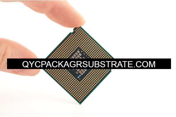
Chip-scale package Substrate Manufacturer and package substrate manufacturer. We use advanced Msap and Sap technology, High multilayer interconnection substrates from 2 to 20 layers.
A Chip-Scale Package (CSP) represents a specialized packaging technology crafted for integrated circuits (ICs), strategically designed to shrink size while preserving essential functionalities and safeguarding the semiconductor chip. CSPs find their niche in applications where spatial constraints are critical, particularly in the realm of compact electronic devices.
Distinctive features characterizing Chip-Scale Packages include:
Diminutive Dimensions: CSPs are meticulously engineered to be remarkably small, often aligning closely with the size of the semiconductor chip itself. This involves a concerted effort to minimize the use of packaging materials and optimize spatial utilization on the Printed Circuit Board (PCB).
Sleek Profile: CSPs are inclined to possess a low profile, signifying minimal elevation above the PCB. This attribute contributes to maintaining a sleek and slender design for electronic devices.
Concise Interconnections: CSPs commonly showcase abbreviated interconnection pathways in comparison to conventional packaging methods. This trait can translate to heightened electrical performance and refined signal integrity.
Lightweight Build: The featherlight nature of CSPs is a result of streamlined packaging materials, rendering them suitable for applications where weight considerations take precedence.
Thermal Proficiency: CSPs may manifest improved thermal capabilities relative to their larger counterparts, owing to their reduced size facilitating more effective heat dissipation. Nevertheless, managing heat remains an ongoing challenge in the realm of miniaturized packaging.
Cost Dynamics: CSPs hold promise in potentially curbing material and manufacturing expenses through judicious use of packaging materials. However, the manufacturing intricacies associated with CSPs might introduce complexities that impact overall costs.
The realm of CSPs encompasses diverse types, encompassing Wafer-Level Chip Scale Packages (WLCSP) and Fan-Out Chip on Substrate (FOCoS), each characterized by unique design nuances and manufacturing considerations. The ascendancy of CSPs is underscored by the increasing miniaturization of electronic devices, propelling a demand surge for smaller, more compact components.
What is the Function of Chip-Scale Package (CSP)?
Chip-Scale Packages (CSPs) play a pivotal role in the world of integrated circuits (ICs), orchestrating a sophisticated dance of technology aimed at compactness without compromising essential functions. Let’s unravel the distinct functions and merits of CSPs:
Size Minimization Mastery: CSPs are maestros of size reduction, artfully diminishing the overall footprint of packaged ICs. This artistry involves a meticulous dance with packaging dimensions and a strategic optimization of spatial real estate on the Printed Circuit Board (PCB).
Spatial Ballet: CSPs pirouette across the PCB, choreographing an intricate ballet that allows more components to gracefully waltz within confined spaces. This flexibility proves invaluable in applications where spatial constraints take center stage, as seen in the design of chic portable electronics.
Elegant Low-Profile Ensemble: CSPs don an elegant low-profile ensemble, ensuring a graceful silhouette with minimal height above the PCB. This design finesse contributes to the creation of sleek and slender electronic devices.
Electrical Performance Pas de Deux: CSPs engage in a refined dance of shorter interconnection paths, a duet that results in heightened electrical performance. This dance is crucial for maintaining the rhythm of signal integrity and minimizing signal delay.
Featherlight Flourish: CSPs showcase a featherlight flourish, a result of a carefully curated reduction in packaging material. This lightness on its feet proves advantageous in weight-sensitive applications, whether it’s the grand stage of aerospace or the intimate setting of portable consumer electronics.
Thermal Ballet: Navigating the challenging terrain of heat management in miniaturized packages, CSPs join a thermal ballet. Their smaller size allows for a more nimble dance of heat dissipation, though the choreography of thermal dynamics remains a perpetual consideration.
Economic Waltz: CSPs engage in an economic waltz, potentially reducing material and manufacturing costs. Despite the intricate steps in the manufacturing process, the minimized use of materials can create an economic rhythm that resonates with cost efficiency.
Diverse Packaging Symphony: CSP technology conducts a symphony of diverse packaging options, from the delicate notes of Wafer-Level Chip Scale Packages (WLCSP) to the harmonious arrangement of Fan-Out Chip on Substrate (FOCoS). This symphony allows for a tailored composition to meet the varied needs of different applications.
In essence, Chip-Scale Packages emerge as the conductors of a harmonious orchestra, orchestrating smaller, lighter, and spatially optimized electronic devices while ensuring the melody of performance and functionality from the encapsulated integrated circuits.
What Are the Different Types of Chip-Scale Package (CSP)?
Chip-Scale Packages (CSP) emerge in an array of forms, each intricately designed to cater to specific nuances in design and manufacturing. Let’s explore some distinctive variations:
Wafer-Level Chip Scale Package (WLCSP):
Description: WLCSP takes center stage in packaging at the wafer level before individual chips take their solo roles.
Advantages: It dances gracefully with a compact form closely mirroring the semiconductor wafer, making it a star in high-density integration.
Applications: Frequently gracing the limelight in mobile devices like smartphones and tablets.
Fan-Out Chip on Substrate (FOCoS):
Description: FOCoS conducts an elegant rearrangement of individual chips on a substrate, allowing for a harmonious flexibility in component arrangement.
Advantages: Its flexibility takes the lead, twirling with enhanced thermal dynamics and the potential for a refined electrical performance.
Applications: Takes a graceful leap into applications demanding a fluidic dance of component placement, particularly in the realm of high-performance computing.
Chip-on-Board (COB):
Description: COB adopts a minimalist choreography, with the semiconductor chip making a direct connection with the PCB without the fuss of additional packaging layers.
Advantages: Celebrates simplicity in its packaging routine, orchestrating cost reductions and potentially enhancing thermal efficiency.
Applications: Finds its rhythm in scenarios where cost considerations take the lead, such as the understated stages of industrial and automotive electronics.
CSP BGA (Ball Grid Array):
Description: CSP BGA entwines the chip in a snug arrangement, featuring solder balls in a symmetrical grid beneath for a symphony of surface mounting.
Advantages: Performs a reliable duet with compactness and efficient thermal dynamics.
Applications: Takes a prominent role in the grand performances of consumer electronics, networking equipment, and the intricate choreography of automotive applications.
Quad Flat No-Lead (QFN):
Description: QFN steps onto the scene as a surface-mount maestro, showcasing a flat bottom without the traditional extensions.
Advantages: Strikes a harmonious chord with compactness, commendable thermal performance, and the simplicity of manufacturing.
Applications: Gracefully weaves into the fabric of integrated circuits and microcontrollers with its versatile performance.
Plastic Chip Carrier (PCC):
Description: PCC, a stalwart in the ensemble, is a plastic chip carrier providing both protection and electrical connections for the chip.
Advantages: Champions cost-effectiveness, finding resonance in applications where spatial constraints play a supportive role.
Applications: Makes a cameo appearance in the eclectic ensemble of consumer electronics, industrial machinery, and the intricate tapestry of automotive systems.
In this symphony of CSPs, these variations come together to create a harmonious blend that caters to the diverse needs of different applications, showcasing the dynamic evolution of chip packaging technology.
What is the Relationship Between Chip-Scale Package (CSP) and IC Packaging?
Chip-Scale Package (CSP) emerges as a distinctive player within the vast tapestry of integrated circuit (IC) packaging. In the broader canvas of IC packaging, a comprehensive process unfolds—encasing semiconductor chips in protective layers, offering both safeguarding and electrical connectivity. CSP, however, is a specialized facet that takes center stage by prioritizing the reduction of the overall package size, often harmonizing closely with the dimensions of the encapsulated semiconductor chip.
The interplay between CSP and IC packaging unfolds with a nuanced choreography:
Panorama of IC Packaging:
Definition: IC packaging orchestrates a symphony of processes, encapsulating semiconductor chips within protective layers to ensure both electrical connectivity and chip protection.
Diversity: The landscape of IC packaging is rich and varied, employing diverse technologies tailored to meet specific requirements and applications.
CSP as a Niche Maestro in IC Packaging:
Size-Centric Symphony: CSP steps into the spotlight as a specialized form of IC packaging, meticulously designed to minimize overall package size, creating a harmonious alignment with the dimensions of the embedded chip.
Spatial Serenade: The overarching theme of CSP is an emphasis on space efficiency, rendering it particularly adept for applications where spatial constraints play a leading role.
Distinctive Notes of CSP:
Compact Crescendo: CSPs are characterized by a compact form, featuring minimal packaging material, concise interconnections, and a low profile above the Printed Circuit Board (PCB).
Direct Integration Duets: Certain CSP variants, including the likes of Wafer-Level Chip Scale Packages (WLCSP), engage in a direct integration ballet at the wafer level before the chips gracefully part ways.
Harmonizing with Industry Dynamics:
Miniaturization Melody: Echoing the broader trend of miniaturization in electronic devices, CSP takes its place as a responsive instrument, attuned to the evolving needs of the electronics industry.
Technological Crescendo: The evolution of CSP mirrors the ongoing symphony of advancements in packaging technologies, harmonizing with the dynamic landscape of contemporary electronic devices.
Application-Specific Crescendos:
Versatile Orchestration: While CSP displays versatility across applications, its crescendo may reach its zenith in scenarios where spatial constraints command attention, such as the realms of smartphones, wearables, and other compact electronic devices.
Synergies in Harmony: CSP, like a seasoned conductor, may elegantly coalesce with other IC packaging technologies, creating a harmonious composition tailored to the intricate requirements of specific applications.
In essence, Chip-Scale Package emerges as a virtuoso, delivering a focused and specialized performance within the grandeur of IC packaging. Its repertoire accentuates compactness, efficiency, and adaptability—a responsive melody in tune with the nuanced demands of contemporary electronic devices.
What are the Differences Between Chip-Scale Package (CSP) and PCB?
Chip-Scale Package (CSP) and Printed Circuit Board (PCB) are distinct entities in the realm of electronics, each carrying out specific functions. Let’s explore the differences between CSP and PCB in a new light:
Unique Profiles:
CSP: Chip-Scale Package is a specialized technology honed for the packaging of integrated circuits (ICs). Its core mission is to shrink size, optimize spatial use, and safeguard the integrity of individual semiconductor chips.
PCB: Printed Circuit Board stands as the structural backbone, fashioned from insulating material with conductive traces. It provides the platform for mounting diverse electronic components and establishing crucial electrical connections.
Operational Focus:
CSP: CSP’s primary mission revolves around encapsulating and shielding individual semiconductor chips. It ensures seamless electrical connections and aims to finesse package size for efficient integration into electronic devices.
PCB: PCB assumes the mantle of the system’s structural foundation, orchestrating the mounting and interconnection of a myriad of electronic components. It acts as the canvas for assembling the entire electronic ensemble.
System Integration Dynamics:
CSP: In the electronic tapestry, CSP plays a pivotal role in packaging and securing individual ICs. It seamlessly integrates into the larger electronic framework, often finding a direct home on the PCB.
PCB: PCB takes center stage as the central structural hub, accommodating and interconnecting diverse electronic elements. It establishes the fundamental architecture of the electronic system.
Compact Craftsmanship:
CSP: Crafted for compactness, CSP finely tailors its size to align with semiconductor chips. Its forte lies in minimizing the overall footprint, making it a go-to choice for applications where size is a critical factor.
PCB: PCBs showcase versatility in size, adapting to the intricacies of electronic systems. They span from petite boards in consumer electronics to expansive boards in industrial settings.
Component Diversity:
CSP: Specializing in semiconductor chips, CSP excels in encapsulating and preserving the integrity of individual ICs.
PCB: PCB hosts a diverse ensemble of electronic components—ICs, resistors, capacitors, connectors, and more. It acts as a unified platform for the integration of this diverse electronic cast.
Interwoven Connectivity:
CSP: CSP focuses on internal interconnections within the package, ensuring a seamless electrical tapestry between the semiconductor chip and external elements.
PCB: PCB orchestrates the interconnections among various electronic components through a network of conductive traces, conducting the harmonious flow of electrical signals.
In essence, Chip-Scale Package emerges as a specialist, safeguarding semiconductor chips with a focus on compactness, while the Printed Circuit Board takes on the role of the foundational conductor, managing the integration and connectivity of a diverse array of electronic components. Together, they compose the essential symphony of electronic devices.
What is the Main Structure and Production Technologies of Chip-Scale Package (CSP)?
The Chip-Scale Package (CSP) emerges as a testament to the artistry of compact design, seamlessly integrating with the semiconductor chip it houses. Its structural components and production technologies weave a narrative of precision and efficiency:
Die Attach:
Description: The semiconductor chip is intricately affixed directly to the package substrate or carrier.
Technology: A palette of methods, from adhesive bonding to soldering and advanced techniques, shapes the delicate dance of die attach.
Package Substrate:
Description: The substrate forms the canvas, providing a stable platform for the semiconductor chip and establishing the ballet of electrical connections.
Technology: Diverse substrates, crafted from organic laminates to advanced ceramics, add layers to the symphony, each chosen with consideration for factors like thermal performance and cost.
Wire Bonding or Flip-Chip Bonding:
Description: Wire bonding delicately strings the semiconductor chip to the package substrate with fine wires, while flip-chip bonding opts for a wire-free rendezvous.
Technology: Fine wires, reminiscent of artistic strokes, are composed of materials like gold or aluminum. Flip-chip bonding, a dance of solder bumps, brings a touch of direct elegance.
Encapsulation or Molding:
Description: The semiconductor chip and wire bonds are gracefully embraced in a protective cocoon through encapsulation or molding, shielding them from environmental elements and the rigors of performance.
Technology: Epoxy resins or molding compounds, akin to the sculptor’s clay, are selected for their role in the grand masterpiece, guided by considerations of thermal conductivity and mechanical properties.
Solder Balls or Bumps:
Description: Solder balls or bumps grace the underbelly, ushering in the CSP’s performance on the stage of a Printed Circuit Board (PCB).
Technology: Solder balls, born from lead-based or lead-free solder materials, engage in a choreography of reflow soldering techniques, ensuring a seamless connection.
Underfill (optional):
Description: Some CSPs choose an underfill performance, filling the interstitial spaces between the semiconductor chip and the package substrate to enhance stability.
Technology: The underfill, a liquid virtuoso in epoxy, transforms into a solid guardian, adding a nuanced layer to the performance.
Thin Profile:
Description: The CSP’s defining feature is its slim silhouette, a harmonious balance above the PCB, navigating the constraints of spatial landscapes.
Technology: Achieving this thin profile is a choreographed engineering feat, a dance of package components and materials, creating a masterpiece of form and function.
In the symphony of CSP production, precision takes the baton, guiding advanced assembly and packaging techniques. Processes like die bonding, wire bonding or flip-chip bonding, encapsulation or molding, and the application of solder balls are performed with the finesse of artists, ensuring the CSP’s reliability and performance. The continuous evolution of manufacturing technologies contributes to an evolving crescendo of improvements in size, performance, and cost-effectiveness within the realm of CSP production.
FAQs
What Varieties of CSPs Do Manufacturers Create?
Answer: CSP manufacturers often offer a range of Chip-Scale Packages, including different sizes, configurations, and technologies. This diversity may include fan-out CSP, flip-chip CSP, and other variations tailored to specific applications.
Which Materials Are Utilized in CSP Manufacturing?
Answer: CSPs are typically crafted using materials such as organic substrates (like laminate), advanced ceramics, epoxy resins for encapsulation, and solder materials for components like solder balls or bumps.
Do CSP Manufacturers Allow Customization?
Answer: Many CSP manufacturers provide customization options to meet the specific requirements of their clients. This can involve tailoring aspects such as size, shape, and packaging technology.
How Critical is Quality Control in CSP Manufacturing?
Answer: Quality control is paramount in CSP manufacturing to ensure the reliability and performance of the final product. Manufacturers implement rigorous testing and inspection procedures to meet industry standards.
What Impact Does Location Have on CSP Manufacturing?
Answer: The location of a CSP manufacturer can influence factors such as shipping costs, lead times, and communication efficiency. Proximity to the manufacturer may be a consideration for companies seeking more responsive support.
Conclusion
To sum up, the Chip-Scale Package (CSP) manufacturing arena is a vibrant fusion of intricate engineering and technological ingenuity. Manufacturers in this field play a pivotal role in sculpting the landscape of integrated circuit packaging, delivering solutions that are not only compact but also highly efficient, tailored to diverse industries. The adaptability ingrained in CSPs, complemented by a spectrum of materials and customization options offered by manufacturers, accentuates the need for a discerning selection process.
At the heart of the narrative in CSP manufacturing is the unwavering commitment to quality control, acting as the cornerstone for ensuring the steadfast reliability and performance of these diminutive yet potent devices. The evolving industry trends, marked by an escalated focus on environmental sustainability and the exploration of avant-garde technologies, point towards a future where CSPs will continue to redefine the boundaries of miniaturization and seamless integration.
In the pursuit of the ideal CSP manufacturer, companies are well-advised to weigh critical factors such as reputation, experience, and a resolute commitment to stringent quality standards. The geographical influence on manufacturing considerations, coupled with the dynamic trajectory of the industry, underscores the necessity for a strategic and well-informed decision-making process.
Fundamentally, the realm of CSP manufacturing unfolds as a symphony where artistry and precision converge to craft compact, high-performance electronic solutions. As technology propels forward, CSP manufacturers stand as pioneers, shaping the panorama of integrated circuits and contributing to the unfolding narrative of electronic devices.