
Cross blind/buried vias PCB manufacturing
Cross blind/buried vias PCB manufacturing,Multilayer HDI PCB supplier. we offer Cross blind/buried vias HDI PCB from 4 layer to 50 layers. Our PCB factory has more than 10000 employees. we offer high qulaity Cross blind/buried vias HDI PCBs or BGA substrates.
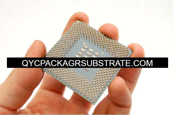
A Cross blind/buried vias PCB is a high-density, high-performance printed circuit board (PCB) design solution commonly used in complex electronic devices. This design employs blind and buried via technologies to maximize connections between different layers of the PCB while minimizing space occupation. Blind vias refer to holes visible only on one side, while buried vias are holes completely embedded within the PCB. By employing cross-layer routing, blind and buried vias can traverse between different layers, enabling more intricate circuit connections and enhancing the PCB’s performance and reliability. This design not only reduces the size of the PCB but also lowers signal transmission delay and improves signal integrity. Consequently, Cross blind/buried vias PCB has become the preferred design solution for many high-end electronic products such as smartphones, tablets, and high-performance computers.
What is a Cross Blind/Buried Vias PCB?
A Cross Blind or Buried Vias PCB (Printed Circuit Board) is a type of PCB design that involves the use of vias, which are essentially small holes drilled into the board that allow electrical connections between different layers of the PCB.
In a traditional PCB design, vias typically run from one surface of the board to another, connecting traces on different layers. However, in a Cross Blind or Buried Vias PCB, the vias are buried within the inner layers of the board, rather than extending all the way through it.
A Cross Blind Via connects traces on adjacent layers, while a Buried Via connects traces on non-adjacent inner layers. This design allows for more complex routing of traces and greater density of components on the surface layers of the board, as the vias do not occupy space on the outer layers.
This type of PCB design is often used in high-density applications where space is limited and signal integrity is critical, such as in smartphones, tablets, and other portable electronic devices. However, it is more complex and costly to manufacture compared to traditional PCB designs due to the additional processes involved in creating the buried vias.
Cross blind/buried vias PCB manufacturing
What are the Cross Blind/Buried Vias PCB Design Guidelines?
Here are some general design guidelines for Cross Blind/Buried Vias PCB:
- Layer Stackup: Plan your layer stackup carefully. Identify which layers will have buried vias and cross blind vias. Ensure that there is proper insulation between adjacent layers to prevent signal interference.
- Via Placement: Strategically place vias to minimize signal path lengths and reduce impedance mismatches. Use simulation tools to analyze signal integrity and optimize via placement.
- Via Size and Pad Design: Ensure that the via sizes are appropriate for the current carrying capacity and signal requirements. Pay attention to pad sizes and shapes to facilitate proper soldering and ensure reliable connections.
- Clearance and Annular Rings: Maintain adequate clearance between vias and other features such as traces, pads, and components to prevent short circuits. Ensure that annular rings (the copper rings around vias) meet minimum requirements for reliability.
- Routing Constraints: Consider routing constraints imposed by the presence of buried and blind vias. Avoid routing traces over vias whenever possible to minimize signal distortion and crosstalk.
- Thermal Considerations: Take into account the thermal effects of buried vias, especially in high-power applications. Ensure that the board’s thermal management system adequately dissipates heat from buried vias to prevent overheating.
- Manufacturability: Collaborate closely with your PCB manufacturer to ensure that the design is manufacturable. Understand their capabilities and limitations regarding buried and blind via fabrication, drilling, and plating processes.
- Testing and Validation: Perform thorough testing and validation of the PCB design, including signal integrity analysis, impedance matching, and thermal testing. Use prototype iterations to refine the design and address any issues that arise.
By following these guidelines and best practices, you can design Cross Blind/Buried Vias PCBs that meet your performance, reliability, and manufacturability requirements.
What is the Cross Blind/Buried Vias PCB Fabrication Process?
The fabrication process for Cross Blind/Buried Vias PCB involves several steps, which may vary slightly depending on the specific requirements of the design and the capabilities of the PCB manufacturer. Here is a general overview of the process:
- Design: The PCB design is created using PCB design software, specifying the placement of components, routing of traces, and the location of Cross Blind and/or Buried Vias.
- Layer Stackup: The layers of the PCB are prepared according to the design requirements. This involves selecting the appropriate materials for each layer and arranging them in the desired sequence.
- Drilling: For Buried Vias, after laminating the layers together, precision drilling is done to create the via holes within the inner layers of the PCB stack. Cross Blind vias are typically drilled after each layer is individually laminated.
- Via Filling (Optional): In some cases, especially for Buried Vias, the via holes may be filled with conductive material to improve electrical conductivity and reliability. This process may involve filling the vias with copper plating or epoxy resin.
- Plating: A thin layer of copper is deposited onto the walls of the drilled via holes through a process called electroplating. This ensures good electrical conductivity and connectivity between layers.
- Lamination: The individual layers of the PCB stack, including any buried vias, are laminated together under heat and pressure to form a single solid board.
- Etching and Tracing: The outer layers of the PCB are coated with a photo-sensitive material called resist, and the desired traces and features are transferred onto the resist layer using photolithography. The exposed copper is then etched away, leaving behind the desired traces.
- Surface Finishing: Surface finishing processes such as HASL (Hot Air Solder Leveling), ENIG (Electroless Nickel Immersion Gold), or OSP (Organic Solderability Preservative) may be applied to improve solderability and protect the exposed copper traces.
- Final Inspection and Testing: The finished PCB undergoes thorough inspection and testing to ensure it meets the specified requirements for dimensional accuracy, electrical connectivity, and reliability.
- Assembly: Components are then soldered onto the PCB using surface mount or through-hole assembly processes to complete the assembly of the electronic circuit.
Throughout the fabrication process, strict quality control measures are implemented to ensure the integrity and reliability of the Cross Blind/Buried Vias PCB. Collaboration between the PCB designer and manufacturer is crucial to address any design considerations and ensure successful fabrication.
How do you manufacture a Cross Blind/Buried Vias PCB?
Manufacturing a Cross Blind/Buried Vias PCB involves several specialized steps to create the buried or blind vias within the layers of the PCB stack. Here’s a general outline of the manufacturing process:
- Design Preparation: Begin with a PCB design that includes the placement of components, routing of traces, and specifications for Cross Blind and/or Buried Vias.
- Layer Stackup Design: Determine the layer stackup based on the design requirements. Identify which layers will contain buried vias and the desired interconnection scheme.
- Preparation of Inner Layers:
– Start by preparing the inner layers of the PCB stack. This may involve laminating together several layers of pre-preg (pre-impregnated fiberglass) and copper foil.
– Drill holes for the buried vias using precision drilling equipment. These holes should be carefully aligned with the via locations specified in the design.
- Via Creation:
– For Buried Vias: After drilling, fill the holes with conductive material such as copper plating or epoxy resin to ensure electrical connectivity.
– For Cross Blind Vias: Drill holes through each individual layer of the PCB stack, ensuring that the holes only penetrate a subset of the layers.
- Copper Plating:
– Electroplate the walls of the drilled holes with a thin layer of copper to establish electrical connectivity between layers.
- Lamination:
– Stack the prepared inner layers together with any additional layers (such as outer layers) and pre-preg material.
– Apply heat and pressure to laminate the layers together, bonding them into a single solid board.
- Outer Layer Processing:
– Prepare the outer layers of the PCB for trace routing and component placement.
– Apply a photo-sensitive resist layer and transfer the trace patterns onto the resist using photolithography.
– Etch away the exposed copper to create the desired traces and features on the outer layers.
- Surface Finishing:
– Apply surface finish to protect exposed copper and improve solderability. Common surface finishes include HASL (Hot Air Solder Leveling), ENIG (Electroless Nickel Immersion Gold), or OSP (Organic Solderability Preservative).
- Final Inspection and Testing:
– Inspect the finished PCB for dimensional accuracy, via integrity, and electrical connectivity.
– Perform electrical testing to ensure that all connections are properly functioning.
- Assembly:
– Once the PCB passes inspection, components can be assembled onto the board using surface mount or through-hole assembly techniques.
Throughout the manufacturing process, quality control measures are implemented to ensure the integrity and reliability of the Cross Blind/Buried Vias PCB. Collaboration between the PCB designer and manufacturer is essential to address any design considerations and ensure successful fabrication.
How much should a Cross Blind/Buried Vias PCB cost?
The cost of manufacturing a Cross Blind/Buried Vias PCB can vary significantly depending on various factors such as the complexity of the design, the number of layers, the size of the board, the quantity ordered, the materials used, and the capabilities of the PCB manufacturer. Here are some factors that can influence the cost:
- Complexity of the Design: Designs with a high density of components, intricate routing, and multiple buried or blind vias will generally cost more to manufacture due to the increased processing time and complexity.
- Number of Layers: PCBs with more layers typically cost more to manufacture than those with fewer layers. Cross Blind/Buried Vias PCBs often involve additional layers to accommodate the buried or blind vias, which can contribute to higher costs.
- Size of the Board: Larger boards require more materials and processing time, which can drive up the manufacturing cost. Smaller boards may be more cost-effective to manufacture.
- Quantity Ordered: Manufacturers often offer volume discounts for larger order quantities. Ordering larger quantities of Cross Blind/Buried Vias PCBs can help reduce the cost per unit.
- Materials Used: The choice of materials for the PCB stackup, such as substrate materials and copper thickness, can affect the cost. High-performance materials or specialty materials may come at a higher price.
- Manufacturing Capabilities: PCB manufacturers with advanced capabilities for drilling, plating, and laminating buried or blind vias may charge higher prices for their services.
- Lead Time: Expedited manufacturing services typically come at a premium cost compared to standard lead times. Planning ahead and allowing for longer lead times can help reduce manufacturing costs.
- Additional Services: Additional services such as surface finishing, panelization, and electrical testing may incur extra costs.
As a rough estimate, the cost of manufacturing a Cross Blind/Buried Vias PCB can range from a few dollars for simpler designs to several hundred dollars or more for complex, high-density designs with advanced features. It’s advisable to obtain quotes from multiple PCB manufacturers to compare costs and find the best value for your specific requirements.
What is the Cross Blind/Buried Vias PCB base material?
The base material for Cross Blind/Buried Vias PCBs typically consists of layers of substrate material laminated together. The choice of base material depends on factors such as the electrical properties, thermal performance, mechanical strength, and cost requirements of the specific application.
Common base materials used in Cross Blind/Buried Vias PCBs include:
- FR-4 (Flame Retardant 4): FR-4 is the most widely used substrate material for PCBs due to its excellent electrical insulation properties, mechanical strength, and affordability. It consists of woven glass fabric impregnated with an epoxy resin.
- High-Tg FR-4: High-Tg (glass transition temperature) FR-4 is a variation of FR-4 with a higher Tg value, which provides better thermal stability and reliability, especially for applications with elevated temperatures.
- Polyimide (PI): Polyimide is a flexible and heat-resistant material suitable for flexible PCBs and applications requiring high-temperature operation. It is commonly used in aerospace, automotive, and medical electronics.
- Rogers and Taconic Laminates: Specialty laminates from manufacturers such as Rogers Corporation and Taconic provide enhanced electrical performance, low dielectric loss, and controlled impedance for high-frequency applications.
- Metal-Core PCBs: For applications requiring efficient heat dissipation, metal-core PCBs with aluminum or copper substrates are used. These are suitable for LED lighting, power electronics, and thermal management applications.
- Ceramic-Based PCBs: Ceramic substrates offer excellent thermal conductivity and reliability, making them suitable for high-power and high-frequency applications where thermal management is critical.
The choice of base material depends on the specific requirements of the PCB design, such as operating conditions, signal integrity, thermal management, and cost considerations. PCB designers typically select the base material that best balances these factors to meet the performance and reliability requirements of the application.
Which company makes Cross Blind/Buried Vias PCB?
Currently, many well-known PCB manufacturing companies offer production services for Cross Blind/Buried Vias PCBs. Some of these companies include (but are not limited to): Eurocircuits, Sanmina, Benchmark Electronics, Advanced Circuits, and Jabil, among others. These companies have advanced manufacturing equipment and professional teams capable of meeting various Cross Blind/Buried Vias PCB manufacturing needs.
Our company also provides Cross Blind/Buried Vias PCB manufacturing services. We have advanced manufacturing equipment and an experienced technical team to meet customers’ requirements for high-quality, complex PCB designs. Our manufacturing process strictly follows industry standards and includes the following key steps:
Design Review: Our team carefully reviews the design files provided by the customer to ensure they meet manufacturing requirements and provides necessary recommendations and improvements.
Material Procurement: We select high-quality PCB base materials to ensure they meet the technical requirements and performance specifications of our customers.
Manufacturing Process Control: We employ advanced manufacturing equipment and stringent process controls to ensure the quality and stability of the PCBs.
Quality Inspection: We conduct rigorous quality inspections, including visual inspection, dimension measurement, electrical testing, etc., to ensure each PCB meets customer requirements and standards.
Timely Delivery: We are committed to delivering customer orders on time to ensure their production schedules are not affected.
Whether it’s a simple double-layer PCB or a complex multi-layer Cross Blind/Buried Vias PCB, we can provide high-quality, reliable production services for our customers. We prioritize communication and collaboration with our customers to provide customized solutions based on their specific requirements and ensure the highest levels of customer satisfaction and product quality.
What are the 7 qualities of good customer service?
Good customer service is characterized by several key qualities that contribute to positive interactions and relationships with customers. Here are seven qualities of good customer service:
- Empathy: Good customer service representatives demonstrate empathy by understanding and acknowledging the customer’s concerns, emotions, and perspectives. They put themselves in the customer’s shoes to better address their needs and provide appropriate support.
- Responsiveness: Good customer service is prompt and responsive. Representatives acknowledge customer inquiries or issues promptly and provide timely assistance or solutions. They strive to minimize wait times and keep customers informed throughout the process.
- Communication Skills: Effective communication is essential for good customer service. Representatives should be clear, courteous, and articulate in their interactions with customers, whether it’s through verbal communication, written correspondence, or digital channels.
- Product Knowledge: Good customer service representatives possess comprehensive knowledge about the products or services they support. They can answer customer questions accurately, provide relevant information, and offer helpful recommendations or troubleshooting guidance.
- Problem-Solving Ability: Good customer service involves the ability to resolve customer issues effectively and efficiently. Representatives should be resourceful, adaptable, and proactive in identifying and addressing customer concerns to achieve satisfactory outcomes.
- Professionalism: Good customer service is conducted with professionalism and integrity. Representatives maintain a positive attitude, remain calm under pressure, and handle challenging situations with grace and respect. They prioritize customer satisfaction while upholding company policies and values.
- Follow-Up and Feedback: Good customer service doesn’t end with the resolution of an immediate issue. Representatives follow up with customers to ensure that their needs have been met and to gather feedback on their experience. They use this feedback to continuously improve service delivery and enhance the overall customer experience.
By embodying these qualities, businesses can build trust, loyalty, and satisfaction among their customers, ultimately fostering long-term relationships and driving success.
FAQs
What are Cross Blind/Buried Vias PCBs?
Cross Blind/Buried Vias PCBs are types of printed circuit boards that utilize buried or blind vias for interconnecting different layers of the PCB. Cross Blind Vias connect traces on adjacent layers, while Buried Vias connect traces on non-adjacent inner layers.
What are the advantages of Cross Blind/Buried Vias PCBs?
Cross Blind/Buried Vias PCBs allow for higher component density, improved signal integrity, and better thermal management compared to traditional PCBs. They also offer enhanced design flexibility and can reduce signal distortion and crosstalk.
What are the applications of Cross Blind/Buried Vias PCBs?
Cross Blind/Buried Vias PCBs are commonly used in high-density electronic devices such as smartphones, tablets, laptops, and medical devices. They are also suitable for applications where space is limited, and signal integrity is critical.
How are Cross Blind/Buried Vias PCBs manufactured?
Manufacturing Cross Blind/Buried Vias PCBs involves specialized processes such as drilling, via filling (for buried vias), plating, lamination, and surface finishing. These processes require advanced equipment and expertise to ensure proper alignment and connectivity between layers.
What design considerations are important for Cross Blind/Buried Vias PCBs?
Design considerations for Cross Blind/Buried Vias PCBs include layer stackup, via placement, via size and pad design, routing constraints, thermal management, and manufacturability. It’s crucial to work closely with PCB designers and manufacturers to optimize the design for performance and reliability.
What are the cost implications of Cross Blind/Buried Vias PCBs?
Cross Blind/Buried Vias PCBs are generally more expensive to manufacture compared to traditional PCBs due to the additional processes involved in creating buried or blind vias. The cost depends on factors such as design complexity, materials used, and order quantity.
How can I ensure the quality of Cross Blind/Buried Vias PCBs?
To ensure the quality of Cross Blind/Buried Vias PCBs, it’s essential to partner with a reputable PCB manufacturer with experience in producing complex PCBs. Quality control measures, including inspections, testing, and adherence to industry standards, should be implemented throughout the manufacturing process.