
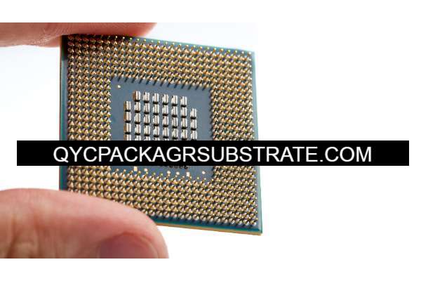
What is DIP Package Substrate?
DIP Package Substrate Service.High speed and high frequency material packaging substrate manufacturing. Advanced packaging substrate production process and technology
A DIP (Dual In-line Package) substrate refers to the physical structure on which integrated circuit (IC) chips or electronic components are mounted. The DIP package substrate typically consists of a flat, rectangular or square-shaped board with metal leads or pins extending from its sides, arranged in a dual in-line configuration. These leads or pins are used for connecting the DIP package to a circuit board or other electronic devices.
The substrate material is usually made of a non-conductive material such as fiberglass epoxy resin, ceramic, or plastic, which provides mechanical support and electrical insulation for the components mounted on it. The leads or pins are typically made of metal such as copper or brass, which facilitate electrical connections between the DIP package and the external circuitry.
DIP packages were commonly used for IC chips and electronic components in the past, but they have largely been replaced by surface mount technology (SMT) packages in many modern electronic devices due to their smaller size and better performance in high-density applications. However, DIP packages are still used in some applications where through-hole mounting is preferred or where legacy components are still in use.
DIP Package Substrate
What are the functions of DIP Package Substrate?
The functions of DIP package substrate include:
Mechanical support: Serving as the mounting platform for integrated circuit chips or electronic components, the DIP package substrate provides mechanical support to ensure these components are securely fixed together during operation.
Electrical insulation: Typically made of non-conductive materials such as fiberglass epoxy resin, ceramic, or plastic, the substrate effectively isolates electronic components and prevents circuit short circuits.
Lead or pin connections: The edges of DIP package substrates usually extend metal leads or pins used to connect the package to circuit boards or other electronic devices, establishing electrical connections and transmitting signals and power.
Heat dissipation: DIP package substrates can also play a role in heat dissipation, transferring the heat generated by integrated circuit chips to the external environment through thermal conductive materials or design to ensure the components operate at normal temperatures.
Environmental protection: Substrate materials often possess properties such as dust and moisture resistance, protecting internal electronic components from external environmental factors and prolonging their lifespan.
Overall, DIP package substrates serve multiple functions including support, insulation, connection, and heat dissipation, crucial for the stable operation of integrated circuit chips or electronic components.
What are the different types of DIP Package Substrate?
There are several different types of DIP package substrates, each designed to meet specific requirements and applications. Some common types include:
Through-Hole DIP (Dual In-line Package): This is the traditional DIP package where the leads or pins extend through holes in the substrate and are soldered onto a circuit board. Through-hole DIPs are commonly used in various electronic devices and are relatively easy to solder and replace.
Surface Mount DIP: Surface mount DIP packages do not have leads extending through holes; instead, they have surface-mount contacts or terminals that are soldered directly onto the surface of a circuit board. Surface mount DIPs are often smaller and more suitable for automated assembly processes.
Ceramic DIP: These DIP packages use a ceramic substrate instead of the more common fiberglass epoxy resin substrate. Ceramic DIPs offer better thermal performance, higher reliability, and improved electrical properties, making them suitable for high-temperature and high-frequency applications.
Plastic DIP: Plastic DIP packages use a plastic substrate, typically made of materials like high-temperature thermoplastics. They are cost-effective and lightweight but may have lower thermal performance compared to ceramic DIPs.
J-Lead DIP: In J-Lead DIP packages, the leads are bent in the shape of a “J” before extending from the package body. This configuration allows for better thermal expansion characteristics and improved solder joint reliability, making them suitable for applications with temperature variations.
Gull Wing DIP: Gull Wing DIP packages have leads that are bent outward and then turned back toward the body of the package in a shape resembling a seagull’s wings. This configuration facilitates surface mounting onto a circuit board and is commonly used in SMT applications.
These are just a few examples of the different types of DIP package substrates available, each with its own unique characteristics and advantages suited for various electronic applications.
What is the relationship between DIP Package Substrate and IC packaging?
The DIP package substrate plays a crucial role in IC (Integrated Circuit) packaging. IC packaging involves enclosing the semiconductor die (the actual silicon chip containing the electronic circuitry) in a protective package that provides electrical connections and mechanical support. The DIP package substrate is a fundamental component of this packaging process.
Here’s how the DIP package substrate relates to IC packaging:
Mounting Surface: The DIP package substrate serves as the mounting surface for the semiconductor die. The die is typically attached to the substrate using adhesive materials and wire bonding or flip-chip bonding techniques.
Electrical Connections: The DIP package substrate provides the means for making electrical connections between the semiconductor die and the external circuitry. This is typically achieved through wire bonding, where thin wires are used to connect the bond pads on the die to the metal leads or pins on the substrate.
Mechanical Support: In addition to providing electrical connections, the DIP package substrate offers mechanical support to the semiconductor die. It ensures that the die remains securely attached during handling and operation, protecting it from physical damage.
Thermal Management: The DIP package substrate also plays a role in thermal management by providing a path for heat dissipation from the semiconductor die. It may incorporate features such as thermal vias or heat sinks to help dissipate heat generated by the integrated circuitry.
Overall, the DIP package substrate is an integral part of the IC packaging process, providing essential functions such as mounting, electrical connections, mechanical support, and thermal management. The design and materials of the substrate are carefully chosen to meet the specific requirements of the IC package and the intended application.
How does DIP Package Substrate differ from PCB?
DIP Package Substrate and PCB (Printed Circuit Board) serve different but complementary roles in electronic systems. Here are the key differences between them:
Function:
DIP Package Substrate: It primarily serves as a mounting platform for integrated circuit chips (ICs) or electronic components, providing mechanical support, electrical connections, and sometimes thermal management for these components.
PCB: It is a complete board that provides interconnections between electronic components. It supports and electrically connects various electronic components such as ICs, resistors, capacitors, and connectors to form a functional electronic circuit.
Construction:
DIP Package Substrate: Typically consists of a flat, rectangular or square-shaped board with metal leads or pins extending from its sides, usually made of non-conductive materials such as fiberglass epoxy resin, ceramic, or plastic.
PCB: Consists of a substrate material (usually fiberglass epoxy resin or similar) with conductive traces printed or etched onto its surface, forming a network of electrical connections between components mounted on the board.
Components:
DIP Package Substrate: It primarily hosts individual IC chips or discrete electronic components such as transistors, diodes, or capacitors.
PCB: It hosts a variety of electronic components, including ICs, resistors, capacitors, connectors, and more, forming a complete electronic circuit.
Integration:
DIP Package Substrate: Generally used for individual IC chips or discrete components and mounted onto a larger PCB or integrated into electronic assemblies.
PCB: Acts as the main platform for integrating and connecting multiple electronic components to form a complete electronic system or device.
Size and Complexity:
DIP Package Substrate: Usually smaller in size and less complex compared to a full PCB, as it typically hosts only one or a few components.
PCB: Can vary in size and complexity depending on the specific application, ranging from simple single-layer boards to complex multilayer boards with intricate circuitry.
In summary, while both DIP Package Substrate and PCB are essential elements in electronic systems, they serve different roles and have distinct characteristics, with the DIP package substrate focusing on hosting and supporting individual components, while the PCB provides the overall platform for interconnecting and integrating multiple components into functional electronic circuits.
What are the structure and production technology of DIP Package Substrate?
The structure and production technology of DIP (Dual In-line Package) package substrates can vary depending on factors such as the specific application, desired performance characteristics, and manufacturing capabilities. However, here is a general overview of the typical structure and production technology:
Structure:
Substrate Material: The substrate material is usually a non-conductive material such as fiberglass epoxy resin, ceramic, or plastic. This material provides mechanical support and electrical insulation for the components mounted on the substrate.
Metal Leads or Pins: The substrate typically has metal leads or pins extending from its sides. These leads or pins are used for connecting the DIP package to a circuit board or other electronic devices. The leads can be arranged in a dual in-line configuration or other configurations depending on the specific design requirements.
Component Mounting Area: The substrate includes an area where integrated circuit chips (ICs) or other electronic components are mounted. This area may have bonding pads or other features for attaching and connecting the components to the substrate.
Optional Features: Depending on the application, the substrate may include additional features such as thermal vias, heat sinks, or shielding to enhance thermal performance or electromagnetic compatibility (EMC).
Production Technology:
Substrate Fabrication: The substrate is typically fabricated using techniques such as injection molding (for plastic substrates), compression molding (for ceramic substrates), or lamination (for fiberglass epoxy resin substrates). These processes involve shaping the substrate material into the desired form and dimensions.
Lead/Pin Attachment: The metal leads or pins are usually attached to the substrate using techniques such as soldering, press-fitting, or welding. The attachment method depends on factors such as the substrate material, lead/pin material, and desired mechanical strength.
Component Mounting: Integrated circuit chips (ICs) or other electronic components are mounted onto the substrate using techniques such as wire bonding, flip-chip bonding, or surface mount technology (SMT). These processes involve attaching the components to the substrate and making electrical connections between the component leads or pads and the substrate.
Finishing Processes: After component mounting, the substrate may undergo finishing processes such as coating, curing, or testing to ensure proper functionality and reliability.
Overall, the production technology of DIP package substrates involves a combination of material processing, assembly, and testing processes to create substrates that meet the requirements of specific applications.
Frequently Asked Questions (FAQs)
What is a DIP package substrate?
A DIP (Dual In-line Package) package substrate is a physical structure on which integrated circuit chips or electronic components are mounted. It typically consists of a flat, rectangular or square-shaped board with metal leads or pins extending from its sides.
What are the functions of a DIP package substrate?
The functions of a DIP package substrate include providing mechanical support, electrical insulation, lead or pin connections for connecting to external circuitry, heat dissipation, and environmental protection for the components mounted on it.
What are the different types of DIP package substrates?
Common types of DIP package substrates include through-hole DIP, surface mount DIP, ceramic DIP, plastic DIP, J-lead DIP, and gull-wing DIP, each with unique characteristics suited for different applications.
How does a DIP package substrate differ from a PCB?
While both serve important roles in electronic systems, a DIP package substrate primarily hosts individual IC chips or discrete electronic components, providing mechanical support and electrical connections. In contrast, a PCB (Printed Circuit Board) supports and connects various electronic components to form a complete electronic circuit.
What is the relationship between a DIP package substrate and IC packaging?
The DIP package substrate is an integral part of IC packaging, providing a mounting platform, electrical connections, mechanical support, and sometimes thermal management for the semiconductor die or electronic components enclosed within the package.
What is the structure and production technology of a DIP package substrate?
The structure of a DIP package substrate typically includes a substrate material, metal leads or pins, a component mounting area, and optional features such as thermal vias or shielding. Production technology involves substrate fabrication, lead/pin attachment, component mounting, and finishing processes.
Conclusion
In conclusion, DIP (Dual In-line Package) package substrates play a critical role in the packaging and integration of integrated circuit chips (ICs) and electronic components. They provide essential functions such as mechanical support, electrical connections, and sometimes thermal management for the components mounted on them.
DIP package substrates come in various types, including through-hole, surface mount, ceramic, plastic, J-lead, and gull-wing, each tailored to specific application requirements. They differ from PCBs (Printed Circuit Boards), which serve as complete platforms for interconnecting multiple electronic components into functional electronic circuits.
The relationship between DIP package substrates and IC packaging is close, as the substrate serves as a mounting platform within the IC package, facilitating electrical connections and providing support for the semiconductor die or electronic components.
The structure and production technology of DIP package substrates involve substrate fabrication, lead/pin attachment, component mounting, and finishing processes. These processes ensure the substrates meet the requirements of various applications in terms of performance, reliability, and functionality.
Overall, DIP package substrates are essential components in electronic systems, enabling the assembly and operation of a wide range of electronic devices and applications.