
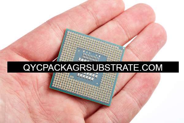
FC-BGA Packaging Substrate maker.Exploring AJINOMOTO’s Cutting-Edge Substrate Materials: ABF Series (GX92R, GXT31R2, GZ41R2H, GL102R8HF)In the realm of advanced materials and technology, AJINOMOTO emerges as a leading innovator, consistently setting new standards in substrate materials. The ABF series, featuring materials such as GX92R, GXT31R2, GZ41R2H, and GL102R8HF, epitomizes AJINOMOTO’s commitment to excellence in the field of electronic materials. This article delves into the key attributes and applications of these cutting-edge substrate materials. by the way. we bought this types materials from Ajinomoto. and built the FC BGA Packaging Substrate with this types base materials.
ABF Series Overview: Unveiling Innovation in Substrate Materials
Introduction: AJINOMOTO’s ABF series, short for “Ajinomoto Build-up Film,” is a testament to the company’s dedication to providing advanced solutions in the realm of substrate materials. These materials serve as the foundation for electronic components and play a pivotal role in ensuring the reliability and performance of electronic devices.
GX92R: High-Performance Build-Up Film for Demanding Applications
Key Features:
- Dielectric Constant Control: GX92R boasts precise dielectric constant control, ensuring optimal signal integrity in high-frequency applications. This makes it suitable for use in advanced communication devices and data transmission systems.
- Thermal Stability: The material exhibits exceptional thermal stability, maintaining its properties even under elevated temperatures. This feature is crucial for applications where thermal management is a critical consideration.
- Low Water Absorption: GX92R’s low water absorption rate contributes to the material’s long-term reliability, making it resistant to environmental factors that could otherwise compromise its performance.
Applications: GX92R finds applications in high-frequency electronic devices, such as antennas, high-speed data communication equipment, and radar systems. Its combination of dielectric performance and thermal stability makes it a go-to choice for demanding electronic applications.
GXT31R2: Flexible Substrate for Bendable Electronics
Key Features:
- Flexibility: GXT31R2 is engineered to be highly flexible, allowing it to bend and conform to the shape of the device. This flexibility is crucial for the development of bendable and wearable electronic products.
- High-Temperature Resistance: The material maintains its integrity even in high-temperature environments, ensuring reliability in applications where temperature fluctuations are common.
- Adhesive Compatibility: GXT31R2 exhibits excellent compatibility with adhesives, facilitating easy integration into various manufacturing processes.
Applications: GXT31R2 is well-suited for flexible electronic applications, including flexible displays, wearable devices, and rollable electronic components. Its flexibility and high-temperature resistance open up new possibilities for design and form factor in the realm of electronic devices.
GZ41R2H: High-Speed Signal Transmission with Enhanced Reliability
Key Features:
- Low Transmission Loss: GZ41R2H is designed for low transmission loss, making it an ideal choice for high-speed signal transmission. This attribute is crucial for maintaining signal integrity in data-intensive applications.
- Dimensional Stability: The material exhibits excellent dimensional stability, ensuring that the substrate maintains its form and properties over time. This stability is vital for applications where precision and reliability are paramount.
- Chemical Resistance: GZ41R2H is resistant to a variety of chemicals, enhancing its durability and reliability in challenging environments.
Applications: GZ41R2H is specifically tailored for high-speed electronic applications, including high-frequency circuit boards, data servers, and communication equipment. Its low transmission loss and dimensional stability make it a key player in the realm of advanced electronic communication.
GL102R8HF: Advanced High-Frequency Substrate for 5G and Beyond
Key Features:
- Ultra-Low Dielectric Constant: GL102R8HF features an ultra-low dielectric constant, making it well-suited for high-frequency applications such as 5G communication. The low dielectric constant minimizes signal loss, ensuring efficient data transmission.
- Excellent Dimensional Accuracy: The material maintains precise dimensional accuracy, contributing to the production of high-performance electronic components with tight tolerances.
- Compatibility with Fine-Line Formation: GL102R8HF is compatible with fine-line formation processes, allowing for the creation of intricate circuit patterns essential for advanced electronic devices.
Applications: GL102R8HF is tailored for high-frequency applications, particularly in the rapidly expanding field of 5G communication. Its ultra-low dielectric constant and compatibility with fine-line formation make it an essential substrate material for the development of advanced communication devices.
Conclusion: Pioneering the Future of Electronic Materials
In conclusion, AJINOMOTO’s ABF series, featuring materials such as GX92R, GXT31R2, GZ41R2H, and GL102R8HF, represents a pinnacle of innovation in substrate materials. These materials address the diverse needs of modern electronic applications, from high-frequency communication devices to flexible and wearable electronics. As technology continues to advance, AJINOMOTO remains at the forefront, driving progress in electronic materials and contributing to the development of the next generation of electronic devices. The ABF series stands as a testament to AJINOMOTO’s commitment to excellence and innovation in the dynamic world of electronic materials.
Importance of Packaging Substrates in Electronic Components
In the ever-evolving world of electronics, where innovation is constant and demands for compact, high-performance devices are on the rise, the role of packaging substrates cannot be overstated. These substrates serve as the critical foundation upon which microchips and semiconductor devices are mounted, connecting them to the broader electronic system. They play a pivotal role in ensuring the reliability, durability, and functionality of these components.
Packaging substrates are the unsung heroes, silently enabling the seamless functioning of our smartphones, computers, automotive electronics, and much more. The choice of substrate profoundly affects factors like electrical performance, thermal management, and overall product size. It’s akin to the foundation of a building, where the right material and design can make the difference between a sturdy structure and a shaky one.
Overview of FCBGA, FCCSP, and Kyocera Substrates
Within the realm of packaging substrates, several innovative solutions have emerged to meet the evolving needs of the electronics industry. Three key players are at the forefront: FCBGA (Flip Chip Ball Grid Array), FCCSP (Flip Chip Chip Scale Package), and Kyocera, a leading company in substrate manufacturing. These substrates have distinct characteristics and advantages, making them essential for various applications.
FCBGA (Flip Chip Ball Grid Array) combines flip chip technology with a ball grid array design, offering enhanced electrical and thermal performance. It has become the go-to choice for many high-end electronic devices.
FCCSP (Flip Chip Chip Scale Package), on the other hand, is known for its compact form factor and high I/O density, making it ideal for applications where space is limited and performance is critical.
Kyocera, a prominent name in the electronics industry, plays a crucial role in substrate development. Their expertise and contributions have shaped the landscape of packaging substrates, facilitating technological advancements in various sectors.
Understanding BGA and Its Variants
What is BGA (Ball Grid Array)?
The Ball Grid Array, or BGA, has long been a cornerstone of semiconductor packaging. It’s a type of surface-mount packaging used to connect integrated circuits (ICs) to printed circuit boards (PCBs). BGA packages are characterized by a grid of small solder balls arranged on the underside of the component. These solder balls serve as both the electrical and mechanical connection to the PCB.
BGA Key Features and Benefits
Key Features and Benefits of Traditional BGA
High I/O Density: BGA packages boast a high input/output (I/O) density due to their compact design. The numerous solder balls facilitate the connection of a significant number of signals in a small area, making them suitable for high-performance applications.
Reliability: BGA’s design results in improved reliability as the solder balls create a strong mechanical connection. They are less susceptible to mechanical stress and vibration, making BGAs a robust choice for products that experience physical wear and tear.
Thermal Performance: The solder balls provide efficient heat dissipation, which is crucial for modern, high-speed microelectronics. The BGA’s thermal performance helps prevent overheating, ensuring the longevity and stability of electronic components.
Comparison between FCBGA and BGA
Now, let’s delve into the differences between the traditional BGA and the more advanced FCBGA:
Flip Chip Technology: While traditional BGA packages rely on wire bonding, FCBGA takes advantage of flip chip technology. In FCBGA, the semiconductor die is flipped upside down and attached directly to the substrate using tiny solder bumps. This results in shorter electrical paths, reducing signal delay and enhancing overall performance.
Substrate Material: BGA packages typically use organic substrates, which are excellent for many applications. In contrast, FCBGA often employs advanced substrates such as silicon, which offer enhanced thermal and electrical properties. This distinction influences the overall performance and capabilities of the package.
Thermal Performance: FCBGA’s unique design, with its direct attachment of the chip to the substrate, enables superior thermal performance compared to traditional BGA. The shorter path for heat dissipation and efficient heat transfer characteristics make FCBGA a preferred choice for devices that demand exceptional thermal management.
Demystifying FCBGA (Flip Chip Ball Grid Array)
Definition and Characteristics of FCBGA
The Flip Chip Ball Grid Array (FCBGA) is a cutting-edge packaging substrate technology that has gained prominence in the electronics industry. At its core, the FCBGA is a specialized integrated circuit packaging solution that combines the benefits of flip chip technology and the reliability of a ball grid array (BGA). This sophisticated packaging method involves mounting the silicon die upside down (flip chip) and connecting it to the substrate using microscopic solder bumps.
Key Characteristics
Flip Chip Technology: Unlike traditional wire bonding, FCBGA employs flip chip technology, where the chip is directly connected to the substrate, reducing the interconnect length and enhancing electrical performance.
Solder Balls: FCBGA packages feature an array of small solder balls on the bottom of the package, which serve as the connections to the circuit board.
High I/O Density: FCBGA provides a high input/output (I/O) density, making it suitable for microprocessors, graphics cards, and other high-performance applications.
Compact Form Factor: The compact design of FCBGA packages saves valuable space on the circuit board, making it ideal for applications with limited real estate.
Enhanced Thermal Performance: The direct connection between the die and the substrate allows for efficient heat dissipation, crucial for high-power devices.
Advantages of FCBGA
FCBGA packaging offers several advantages that have made it a popular choice in the Electronics industry:
High Performance: FCBGA’s shortened interconnects and direct die-to-substrate connections result in improved electrical performance, reduced signal loss, and increased data transfer rates.
Thermal Efficiency: The direct connection between the silicon die and the substrate allows for efficient heat dissipation, ensuring that high-power components can operate reliably without overheating.
Reliability: FCBGA’s solder ball connections provide mechanical robustness, reducing the risk of package cracking or delamination during thermal cycling.
Space-Efficient: FCBGA’s compact form factor makes it an excellent choice for compact electronic devices, as it optimizes the use of space on the circuit board.
Versatility: FCBGA packaging is versatile and well-suited for a wide range of applications, from microprocessors and graphic processors to networking equipment and embedded systems.
FCBGA Packaging Substrate
The FC-BGA Substrate in Detail
In-depth Exploration of the FC-BGA (Flip Chip Ball Grid Array) Substrate
The FC-BGA, or Flip Chip Ball Grid Array, is a remarkable advancement in the world of semiconductor packaging. This substrate offers a sophisticated interconnection technology that has become crucial in modern electronics. Let’s delve deeper into what makes FC-BGA stand out:
Interconnection Methodology: FC-BGA employs the flip chip technology, where the semiconductor die is directly attached to the substrate, forming a face-down connection. This close proximity reduces signal paths, minimizing inductance and enhancing electrical performance.
High I/O Density: FC-BGA boasts a high input/output (I/O) density, meaning it can accommodate a large number of connections in a relatively small footprint. This feature is invaluable in applications where space is limited, such as mobile devices and high-performance computing.
Improved Signal Integrity: Thanks to its compact design and reduced trace lengths, FC-BGA minimizes signal skew and crosstalk, ensuring excellent signal integrity. This is especially critical in applications like high-speed data transfer and processing.
Enhanced Thermal Management: FC-BGA substrates are designed with efficient heat dissipation in mind. This technology aids in maintaining optimal operating temperatures for sensitive components, preventing overheating and ensuring long-term reliability.
Unique Features and Use Cases
FC-BGA’s unique features open the door to a wide array of use cases
Miniaturized Electronics: Due to its small form factor and high I/O density, FC-BGA is the preferred choice for compact electronic devices like smartphones, tablets, and wearable technology.
High-Performance Computing: FC-BGA’s exceptional signal integrity and thermal management make it ideal for use in high-performance computing systems, data centers, and server farms.
Networking Equipment: Networking components often require a high I/O density and reliable interconnections. FC-BGA excels in these scenarios, providing a stable and efficient solution.
Automotive Electronics: FC-BGA’s resistance to temperature fluctuations and its capacity for high-speed data transfer make it a suitable option for automotive control units and infotainment systems.
How FC-BGA Differs from Traditional BGA and FCBGA
To understand the significance of FC-BGA, it’s essential to differentiate it from traditional BGA and FCBGA:
Traditional BGA: Traditional BGAs utilize wire bonding, which involves connecting the semiconductor die to the substrate using wire connections. In contrast, FC-BGA employs flip chip technology, eliminating wire bonds and reducing inductance for improved performance.
FCBGA (Flip Chip BGA): While FC-BGA and FCBGA may sound similar, they differ in their design and purpose. FCBGA typically refers to flip chip technology used in a BGA package, while FC-BGA is a distinct packaging type designed with unique features, such as its high I/O density and thermal management capabilities.
Advantages Over Both: FC-BGA combines the advantages of traditional BGA, such as ease of manufacturing, with the advantages of flip chip technology, such as enhanced performance and thermal management. It bridges the gap between these two packaging methods, making it a versatile and reliable choice for various applications.
In conclusion
The significance of advanced packaging substrates in modern electronics Advanced packaging substrates such as FCBGA and FCCSP play a pivotal role in the development of modern electronics. As the demand for smaller, faster, more efficient electronic devices continues to grow, these substrates provide solutions that enhance performance, reliability and form factor. They are at the heart of innovation in consumer electronics, telecommunications, automotive technology and many other industries.
The use of flip-chip technology and advanced substrate materials, such as those provided by Kyocera, has revolutionized the way electronic components are designed and manufactured. Their compact form factor and high I/O density paves the way for more powerful and versatile devices, enabling the Internet of Things (IoT) and other breakthrough technologies.
In summary, advanced packaging substrates are the unsung heroes behind the impressive electronic devices we use every day. As the electronics world continues to evolve, understanding the latest substrate technologies and partnering with industry leaders like Kyocera is critical to staying at the forefront of innovation and ensuring project success.