
FCBGA Package Vender . The best samllest bump pitch with 90 um, the extra small trace and spacing are 9um/9um. the best smallest via holes size are 50um.
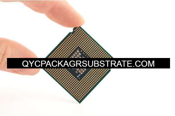
The FCBGA, or Flip-Chip Ball Grid Array, is a type of semiconductor packaging technology used in integrated circuits (ICs) and microprocessors. It is a specific variation of the more general Ball Grid Array (BGA) packaging.
Here are some key features and aspects of the FCBGA package:
Flip-Chip Technology:
In FCBGA, the integrated circuit (IC) is “flipped” upside down and mounted directly onto the substrate or circuit board.
The active side of the IC, which contains the semiconductor die and the electrical connections (bond pads), faces downward.
Ball Grid Array (BGA):
FCBGA belongs to the broader category of Ball Grid Array packages, where the bottom of the package has an array of solder balls that serve as the electrical and mechanical connections to the circuit board.
The solder balls are organized in a grid pattern, enhancing the secure and dependable connection between the integrated circuit (IC) and the circuit board.
Advantages:
Flip-chip technology enhances thermal performance by facilitating more efficient dissipation of heat generated by the integrated circuit. This is achieved through a direct connection to the substrate, enabling effective heat transfer and management.
Shorter Interconnects: The direct connections (shorter interconnects) between the die and the substrate result in improved electrical performance, reduced signal delays, and lower inductance.
Higher Density: FCBGA packages enable higher pin counts and increased component density on the substrate, making them suitable for high-performance applications.
Applications:
FCBGA (Flip-Chip Ball Grid Array) packages are frequently employed in demanding computing applications, including microprocessors, graphics processing units (GPUs), and other intricate integrated circuits. These packages are preferred in such scenarios due to their capability to efficiently manage thermal concerns and deliver superior electrical performance.
Manufacturing Process:
The manufacturing process involves attaching the flipped IC to the substrate using solder bumps or solder balls. This process is typically done using advanced manufacturing equipment.
Challenges:
While FCBGA offers several advantages, its manufacturing process can be more complex and costly. Additionally, the package may be more challenging to inspect and repair due to the placement of the IC on the bottom side.
In summary, the FCBGA package stands out for its use of flip-chip technology, which provides advantages in terms of thermal performance, electrical characteristics, and component density, making it suitable for high-performance electronic devices.
What Functions Does the FCBGA Package Serve?
The FCBGA (Flip-Chip Ball Grid Array) package serves a variety of critical functions that contribute to the overall reliability and performance of integrated circuits. Here’s an exploration of its multifaceted roles:
Enhanced Thermal Performance:
FCBGA excels in dissipating heat generated by integrated circuits. The direct connection between the flip-chip and the substrate allows for efficient heat transfer, preventing overheating and ensuring optimal operating temperatures.
Optimized Signal Integrity:
The flip-chip configuration in FCBGA results in shorter interconnects between the semiconductor die and the substrate. This design minimizes signal delays and reduces inductance, contributing to improved signal integrity and faster data transmission.
Increased Component Density:
FCBGA packages enable higher pin counts and a greater concentration of components on the substrate. This increased density is particularly beneficial for complex integrated circuits, facilitating the design of high-performance devices with a smaller footprint.
Reduced Electromagnetic Interference (EMI):
The compact and well-organized layout of FCBGA helps in minimizing electromagnetic interference. Shorter interconnects and a well-controlled design contribute to lower EMI, enhancing the overall electromagnetic compatibility of the integrated circuit.
Mechanical Reliability:
The solder ball grid array provides a reliable mechanical connection between the integrated circuit and the circuit board. This robust attachment method enhances the overall mechanical stability of the package, reducing the risk of mechanical failures.
Improved Electrical Performance:
FCBGA packages offer superior electrical performance due to the shortened signal paths, lower inductance, and optimized interconnect design. This contributes to reduced signal degradation and improved overall efficiency of the integrated circuit.
Suitability for High-Performance Applications:
Designed to meet the demands of high-performance computing applications, FCBGA packages are commonly used in microprocessors, GPUs, and other sophisticated integrated circuits. Their ability to balance thermal considerations and electrical performance makes them well-suited for such applications.
Advanced Manufacturing Techniques:
The manufacturing process for FCBGA involves advanced techniques for attaching the flip-chip to the substrate, ensuring precision and reliability during production.
In summary, the FCBGA package performs a range of functions, including thermal management, signal integrity optimization, increased component density, reduced EMI, mechanical reliability, improved electrical performance, and suitability for high-performance applications. These functions collectively contribute to the overall reliability and efficiency of integrated circuits in demanding computing environments.
What Are the Different Types of FCBGA Package?
The landscape of FCBGA (Flip-Chip Ball Grid Array) packages includes various types, each designed with unique characteristics to cater to specific applications within the electronics industry. Here are some of the different types of FCBGA packages along with their distinctive features:
Traditional FCBGA:
This is the standard FCBGA configuration with the flip-chip mounted directly onto the substrate. It offers the basic benefits of enhanced thermal performance, reduced signal delays, and increased component density.
Fine-Pitch FCBGA:
Fine-pitch FCBGA packages have a smaller pitch (distance between solder balls) than traditional FCBGA. This allows for higher pin counts and greater component density, making them suitable for applications where space is a critical factor.
Ultra-Fine-Pitch FCBGA:
Ultra-fine-pitch FCBGA takes miniaturization to the next level, featuring an even smaller pitch than fine-pitch variants. These packages are used in applications demanding the highest level of component integration in a limited space.
High-Bandwidth FCBGA:
High-bandwidth FCBGA packages are specifically engineered to fulfill the needs of applications that require exceptionally rapid data transfer rates. These packages find common use in high-performance computing devices, including graphics processing units (GPUs), where the demand for swift and efficient data processing is paramount.
Power-Optimized FCBGA:
Focused on power efficiency, power-optimized FCBGA packages are designed to minimize energy consumption and heat dissipation. They are commonly used in devices where power efficiency is a critical consideration.
Stacked FCBGA:
Stacked FCBGA packages involve the integration of multiple semiconductor dies on top of each other within a single package. This allows for increased functionality and performance in a compact form factor.
Heterogeneous Integration FCBGA:
These packages incorporate different types of semiconductor materials or technologies within the same package. Heterogeneous integration FCBGA is used to combine the strengths of various materials or processes for enhanced performance.
System-in-Package (SiP) FCBGA:
SiP FCBGA integrates not only the semiconductor die but also other components, such as passive elements and even entire subsystems, into a single package. This integration enhances system-level performance and reduces the need for external components.
Multi-Die FCBGA:
Multi-die FCBGA packages involve the integration of multiple semiconductor dies for specific functionalities, offering a modular approach to system design.
Understanding the characteristics and applications of these different FCBGA types is crucial for making informed decisions in electronic component selection. Depending on the specific requirements of a given application, engineers and designers can choose the most suitable FCBGA package to optimize performance, space utilization, and power efficiency.
How Does the FCBGA Package Collaborate with PCBs?
FCBGA Package Integration with PCBs:
Interface with PCBs:
FCBGA packages interface with printed circuit boards (PCBs) through an array of solder balls on the package’s underside. These solder balls create electrical and mechanical connections, facilitating the transfer of signals between the integrated circuit and the PCB.
Challenges and Strategies:
Challenges in integrating FCBGA packages include the precision required during soldering and potential issues with inspection and repair due to the package’s design. Strategies involve advanced manufacturing techniques, such as automated assembly and inspection, to ensure accurate and reliable connections.
Impact on Motherboard Integration:
System Design and Performance:
FCBGA technology significantly impacts motherboard integration by offering improved thermal management and signal integrity. The direct connection of the flip-chip to the substrate enhances overall system performance, making FCBGA packages suitable for high-performance applications like microprocessors and GPUs.
Differentiation Between Substrate and Traditional PCBs:
Role of Substrate vs. PCB:
The substrate used in FCBGA packages serves as the immediate interface between the flip-chip and the PCB. It provides a foundation for mounting the flip-chip and contains the necessary routing and connections. In contrast, a traditional PCB serves as the broader platform for hosting various components and interconnecting them.
Compatibility of FCBGA with SLP and HDI Substrates:
SLP (Substrate-Like PCBs):
SLP substrates share similarities with FCBGA substrates, as both focus on miniaturization and enhanced performance. The compatibility lies in their shared goals of achieving higher component density and improved electrical performance.
HDI (High-Density Interconnect) Substrates:
FCBGA technology aligns well with HDI substrates, as both emphasize compact designs and reduced signal interference. The combination of FCBGA with HDI substrates allows for advanced packaging solutions suitable for high-speed and high-density applications.
In summary, the collaboration between FCBGA packages and PCBs involves precise solder ball connections, posing challenges in manufacturing and inspection. FCBGA’s impact on motherboard integration is substantial, enhancing thermal performance and signal integrity. The substrate in FCBGA plays a crucial role in connecting the flip-chip to the PCB, and it differs from traditional PCBs in its specialized function. The compatibility of FCBGA with SLP and HDI substrates highlights its adaptability to advanced PCB structures, fostering improved electronic assemblies in terms of size, performance, and reliability.
What Constitutes the Main Structure and Production Technologies of FCBGA Package?
Main Structure of FCBGA Package:
Flip-Chip Configuration:
The core structure of FCBGA packages involves a flip-chip configuration, where the semiconductor die is flipped and mounted directly onto the substrate. The active side of the chip, containing the circuitry and bond pads, faces downward.
Solder Ball Grid Array (BGA):
The bottom of the FCBGA package features a grid array of solder balls. These solder balls serve as both electrical and mechanical connections between the integrated circuit and the printed circuit board (PCB).
Substrate:
The substrate plays a critical role in the structure, serving as the interface between the flip-chip and the PCB. It provides a foundation for mounting the flip-chip and contains the necessary routing for electrical connections.
Production Technologies of FCBGA Package:
Improved HDI Fabrication Technology:
High-Density Interconnect (HDI) fabrication technology is a crucial aspect of FCBGA production. This technology enables the creation of intricate multilayered circuits with very fine traces and spaces. Improved HDI fabrication involves advanced techniques to achieve even higher density, facilitating the complex requirements of FCBGA packages.
Improved Semi-Additive Method:
The Improved Semi-Additive Method is an innovative approach in FCBGA production. This method involves selectively depositing and patterning thin layers of conductive material on the substrate. It allows for precise control over the creation of fine features, contributing to the miniaturization and increased component density of FCBGA packages.
Advanced Manufacturing Processes:
FCBGA packages utilize advanced manufacturing processes to attach the flip-chip to the substrate. This often involves precision placement and soldering techniques, such as reflow soldering or controlled collapse chip connection (C4) technology.
Automated Assembly:
Automation plays a significant role in the production of FCBGA packages. Automated assembly lines ensure consistency and accuracy in the placement of flip-chips and solder balls, reducing the risk of errors and enhancing overall production efficiency.
Overall Impact:
Miniaturization and Component Density:
The combination of the flip-chip configuration, solder ball grid array, Improved HDI fabrication, and the Improved Semi-Additive Method contributes to the miniaturization of FCBGA packages. This, in turn, allows for higher component density on the substrate.
Improved Electrical Performance:
The use of advanced production technologies results in FCBGA packages with improved electrical performance. Shorter interconnects, finer traces, and precise manufacturing contribute to reduced signal delays and enhanced signal integrity.
In summary, the main structure of FCBGA packages involves a flip-chip configuration, solder ball grid array, and a crucial substrate. The production technologies include Improved HDI fabrication and the Innovative Semi-Additive Method, along with advanced manufacturing processes and automated assembly. These elements collectively contribute to the miniaturization, increased component density, and improved electrical performance of FCBGA packages.
FAQs: Demystifying FCBGA Package Technology
What is FCBGA, and where is it commonly used?
FCBGA stands for Flip-Chip Ball Grid Array.It is a prevalent semiconductor packaging technology employed in high-performance computing applications, including microprocessors, graphics processing units (GPUs), and various intricate integrated circuits.
What are the advantages of FCBGA packages?
FCBGA packages offer several advantages, including enhanced thermal performance, optimized signal integrity, increased component density, reduced electromagnetic interference (EMI), and improved electrical performance. These features make them suitable for applications requiring high reliability and performance.
How does FCBGA impact motherboard integration?
FCBGA technology positively impacts motherboard integration by providing improved thermal management and signal integrity. The direct connection of the flip-chip to the substrate enhances overall system performance, making FCBGA packages well-suited for high-performance computing devices.
What is the role of the substrate in FCBGA packages?
The substrate in FCBGA packages serves as the immediate interface between the flip-chip and the printed circuit board (PCB). It provides a foundation for mounting the flip-chip and contains the necessary routing for electrical connections.
How is FCBGA different from traditional BGA packages?
FCBGA is a variation of Ball Grid Array (BGA) packaging. The key difference lies in the flip-chip configuration, where the semiconductor die is flipped and mounted directly onto the substrate. This design offers advantages in thermal management, signal integrity, and component density compared to traditional BGAs.
What production technologies are used in FCBGA fabrication?
FCBGA fabrication involves advanced production technologies, including Improved High-Density Interconnect (HDI) fabrication and the Improved Semi-Additive Method. These methods contribute to miniaturization, increased component density, and improved electrical performance.
What challenges are associated with FCBGA technology?
Answer: Challenges in FCBGA technology include the precision required during soldering, potential difficulties in inspection and repair due to the flip-chip configuration, and the complexity of the manufacturing process. Advanced manufacturing techniques and automated assembly are employed to address these challenges.
Are FCBGA packages compatible with advanced PCB structures like SLP and HDI?
Answer: Yes, FCBGA packages are compatible with advanced PCB structures such as Substrate-Like PCBs (SLP) and High-Density Interconnect (HDI) substrates. The combination allows for optimized designs in terms of size, performance, and reliability.
In what applications are FCBGA packages commonly used?
Answer: FCBGA packages are commonly used in high-performance computing applications, including microprocessors, GPUs, and complex integrated circuits where thermal management and electrical performance are crucial.
How does FCBGA contribute to miniaturization in electronic assemblies?
Answer: FCBGA contributes to miniaturization through its flip-chip configuration, solder ball grid array, and advanced production technologies. These features allow for higher component density and smaller form factors in electronic assemblies.
In Conclusion, Can FCBGA Packages Shape the Future of PCB Engineering?
In conclusion, FCBGA (Flip-Chip Ball Grid Array) packages hold the potential to be transformative catalysts for innovation in PCB (Printed Circuit Board) engineering. Beyond their compact form, these packages offer a range of advantages, from enhanced thermal performance to improved signal integrity, making them pivotal components in high-performance computing applications.
The adaptability and efficiency of FCBGA packages position them as key enablers for pushing the boundaries of what is achievable in modern electronic design. Their influence extends beyond conventional packaging methods, contributing to the miniaturization, increased component density, and overall performance enhancement of electronic assemblies.
As technology continues to advance, the integration and optimization of FCBGA packages are expected to play a crucial role in shaping the future landscape of electronic components and integrated circuits. Engineers and designers can leverage the advantages offered by FCBGA technology to meet the evolving demands of cutting-edge applications, fostering innovation and driving progress in PCB engineering. Understanding and harnessing the power of FCBGA packages will be instrumental in staying at the forefront of electronic design and ensuring the development of more powerful, efficient, and compact electronic devices.