
FCBGA Packaging Firm . the Package Substrate will be made with Showa Denko and Ajinomoto High speed materials.or other types high speed materials and high frequency materials.
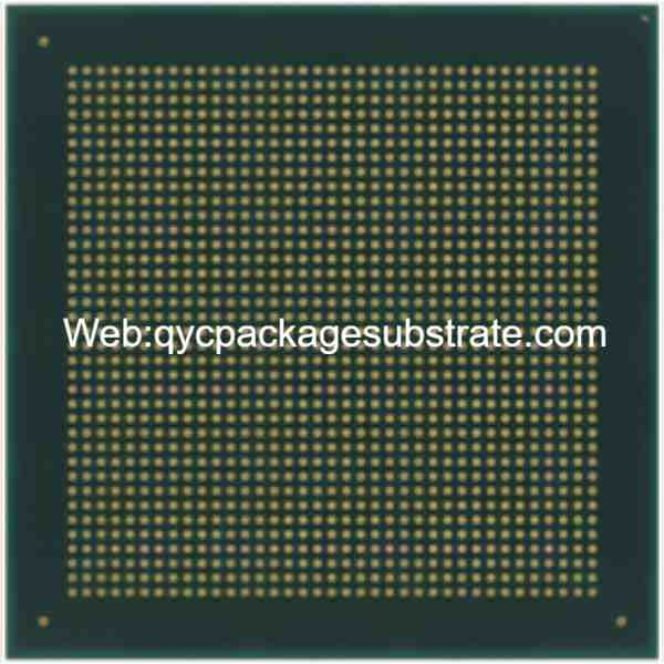
FCBGA stands for Fine-pitch Chip Ball Grid Array.FCBGA (Fine-pitch Chip Ball Grid Array) is a semiconductor packaging technology where a silicon chip is affixed to a substrate. The connection between the chip and the substrate is established through an array of solder balls arranged in a grid pattern on the package’s underside. This configuration enables efficient electrical connections between the chip and the broader electronic system.
The term “fine-pitch” in FCBGA refers to the small pitch or spacing between the solder balls. The close arrangement of solder balls in FCBGA enables a greater concentration of interconnections, making it well-suited for applications that demand numerous connections within confined spaces.
FCBGA (Fine-pitch Chip Ball Grid Array) packaging is extensively employed in diverse electronic devices, such as microprocessors, graphics processing units (GPUs), and various integrated circuits. Its merits encompass enhanced electrical performance, superior thermal dissipation, and a more condensed form factor in contrast to certain alternative packaging technologies.
Whether FCBGA packaging is poised to revolutionize the semiconductor industry depends on the fact that the industry is in a constant state of evolution, with diverse packaging technologies coexisting to meet various requirements. FCBGA is merely one among numerous packaging options within the industry.The choice of packaging technology depends on factors such as the specific application, performance requirements, power considerations, and cost constraints.
While FCBGA packaging offers advantages in terms of density and performance, other packaging technologies like Chip-on-Board (COB), Quad Flat Package (QFP), and others also have their own strengths and use cases. The semiconductor industry often sees incremental advancements in packaging technologies rather than a single revolutionary change.
In summary, FCBGA is a notable packaging technology in the semiconductor industry, and its fine-pitch design contributes to its popularity for certain applications. However, whether it will revolutionize the entire industry depends on the broader landscape of technological advancements and the specific needs of different applications.
What Functions Does FCBGA Serve Beyond Electrical Connections?
FCBGA (Fine-pitch Chip Ball Grid Array) packaging serves functions beyond electrical connections, encompassing several crucial aspects that contribute to its widespread use in modern chip designs. Here are some of the multifaceted functions of FCBGA:
Electrical Connections: The primary function of FCBGA is to establish electrical connections between the silicon chip and the rest of the electronic system. The fine-pitch arrangement of solder balls allows for a high density of interconnections, enabling the efficient transmission of electrical signals.
Heat Dissipation: FCBGA packaging plays a vital role in heat dissipation. As electronic devices continue to become more powerful, managing heat is a critical consideration. The solder balls and the packaging design facilitate efficient heat transfer from the silicon chip to the substrate and, consequently, to the surrounding environment. This helps prevent overheating and ensures the proper functioning of the semiconductor device.
Mechanical Stability: FCBGA packaging provides mechanical stability to the integrated circuit. The solder balls play a crucial role in establishing a strong mechanical link between the silicon chip and the substrate, reinforcing the structural integrity of the package. This is especially significant in scenarios where the device may encounter mechanical stress or vibrations.
Compact Form Factor: The fine-pitch configuration of FCBGA facilitates a more condensed form factor when contrasted with certain alternative packaging choices.This is crucial in applications where space is at a premium, such as in mobile devices and other compact electronic gadgets. The small footprint of FCBGA contributes to the miniaturization of electronic components.
Signal Integrity: FCBGA packaging helps maintain signal integrity by reducing signal interference and crosstalk. The proximity of solder balls in FCBGA packaging minimizes signal path lengths, decreasing the risk of signal degradation. This becomes particularly crucial in high-performance applications where maintaining optimal signal quality is of paramount importance.
High-Density Integration: FCBGA enables high-density integration of electronic components. The fine pitch allows for a large number of connections in a limited space, making it suitable for complex and densely packed semiconductor devices, including microprocessors and GPUs.
In summary, FCBGA packaging serves multiple functions, including electrical connections, heat dissipation, mechanical stability, compact form factor, signal integrity, and high-density integration. These features collectively contribute to meeting the high requirements of modern chip designs, particularly in applications where performance, reliability, and miniaturization are essential considerations.
What Types of FCBGA Packaging Exist in the Market?
Indeed, there are various types of FCBGA (Fine-pitch Chip Ball Grid Array) packaging available in the market. Here’s an overview of some key types and features:
High-Density Interconnect (HDI) Substrates: FCBGA packaging often utilizes High-Density Interconnect substrates. These substrates incorporate advanced technologies to achieve a high density of electrical connections. HDI substrates can include multiple layers of thin traces, vias, and microvias, allowing for more compact and complex circuit designs.
Fine-Pitch Variations: FCBGA packaging comes in different fine-pitch variations. The pitch refers to the distance between the centers of adjacent solder balls. Variations in pitch sizes allow for flexibility in design and application, accommodating different performance and space requirements. Smaller pitches typically enable higher connection densities.
Package-on-Package (PoP): In some cases, FCBGA is used in a Package-on-Package configuration. This involves stacking multiple semiconductor packages on top of each other, connected through interconnects. PoP is commonly employed in mobile devices to integrate different functions, such as a processor and memory, in a compact form factor.
Flip-Chip Configuration: FCBGA often employs a flip-chip configuration, where the active side of the semiconductor die faces down and connects directly to the substrate using solder bumps. This configuration enhances electrical performance, reduces signal path lengths, and improves heat dissipation.
Advanced Substrate Materials: FCBGA packaging may use advanced substrate materials to enhance performance. Materials with high thermal conductivity, such as certain ceramics and metal-core laminates, can be employed to improve heat dissipation and overall reliability.
Differences from Traditional PCBs: FCBGA substrates differ from traditional Printed Circuit Boards (PCBs). They are specifically designed to accommodate the unique requirements of semiconductor packaging. The focus is on optimizing electrical performance, heat dissipation, and mechanical stability rather than serving as a general-purpose board for electronic components.
Technological Features: FCBGA packaging incorporates various technological features to meet the demands of modern applications. This can include features such as built-in power delivery networks, embedded passive components, and specialized materials for improved signal integrity.
In summary, the market offers different types of FCBGA packaging with variations in fine-pitch sizes, substrate materials, and configurations. These variations cater to diverse application needs, ranging from high-performance computing to compact mobile devices, and each type brings specific technological features to enhance the functionality and reliability of semiconductor devices.
How Does FCBGA Compare with Traditional PCBs?
FCBGA (Fine-pitch Chip Ball Grid Array) packaging differs significantly from traditional PCBs (Printed Circuit Boards) in terms of design, application, and functionality. Here’s a breakdown of the disparities:
Design and Structure:
FCBGA: FCBGA is a specialized packaging technology designed specifically for semiconductor devices. It involves mounting a silicon chip on a substrate, with solder balls connecting the chip to the substrate. The fine-pitch arrangement of solder balls allows for a high density of interconnections.
Traditional PCBs: Traditional PCBs serve as the foundation for electronic components on a broad scale. They consist of layers of fiberglass or other insulating materials with copper traces that form the electrical pathways. Components are mounted on the PCB using various methods like through-hole or surface-mount technology.
Applications in Motherboards:
FCBGA: FCBGA packaging is frequently employed for high-performance integrated circuits, notably in CPUs (Central Processing Units) and GPUs (Graphics Processing Units). Its usage in general-purpose components on a motherboard is less common.
Traditional PCBs: Motherboards primarily use traditional PCBs as the base for mounting various components such as processors, memory modules, and peripheral connectors.
High-Density Interconnections:
FCBGA: FCBGA is known for its fine-pitch arrangement, enabling a high density of interconnections between the silicon chip and the substrate. This is particularly advantageous in applications where numerous connections are required in a confined space.
Traditional PCBs: While traditional PCBs can support high-density components, they may not achieve the same level of fine-pitch interconnections as FCBGA.
Customization and Flexibility:
FCBGA: FCBGA is a specialized packaging method optimized for specific semiconductor applications. It offers less flexibility in terms of general-purpose electronic component placement compared to traditional PCBs.
Traditional PCBs: Traditional PCBs are highly versatile and can accommodate a wide range of electronic components and configurations, making them suitable for various applications.
Comparison with Other Forms of Packaging:
FCBGA vs. QFP (Quad Flat Package): FCBGA generally offers higher pin density than QFP, making it suitable for applications requiring more connections in a smaller space.
FCBGA vs. COB (Chip-on-Board): FCBGA is a package type, whereas COB involves directly attaching unpackaged chips to the substrate. FCBGA provides better protection for the chip and allows for a more standardized manufacturing process.
In summary, FCBGA packaging is specialized for high-performance semiconductor devices, offering advantages such as fine-pitch interconnections, efficient heat dissipation, and a compact form factor. Traditional PCBs, on the other hand, are more versatile and widely used for general-purpose electronic components on various devices, including motherboards. The choice between FCBGA and traditional PCB depends on the specific requirements of the application.
What Constitutes the Main Structure and Production Technologies of FCBGA Packaging?
The main structure of FCBGA (Fine-pitch Chip Ball Grid Array) packaging consists of a silicon chip mounted on a substrate, with solder balls forming a grid array on the bottom side. The manufacturing technologies for FCBGA have evolved to meet the challenges posed by advanced electronic products. Two key aspects of this evolution include improved HDI (High-Density Interconnect) manufacturing technology and an enhanced semi-additive method for substrate manufacturing:
High-Density Interconnect (HDI) Manufacturing Technology:
Structure: FCBGA packaging often utilizes HDI substrates, which incorporate advanced manufacturing techniques to achieve a high density of interconnections. HDI substrates may have multiple layers with microvias and thin traces, allowing for intricate circuit designs in a compact space.
Benefits: The use of HDI technology enhances the electrical performance of FCBGA packaging by reducing signal path lengths and supporting a higher density of connections. This is crucial for high-performance applications where signal integrity is paramount.
Enhanced Semi-Additive Method for Substrate Manufacturing:
Structure: The substrate of FCBGA is a key component that supports the silicon chip and facilitates the electrical connections. An enhanced semi-additive method involves selectively adding material to the substrate to create circuit patterns and connections.
Benefits: This method allows for more precise and complex circuitry, contributing to improved electrical performance and reliability. It also supports the miniaturization of the overall package, which is essential for meeting the demands of advanced electronic products with compact designs.
Advanced Materials:
Structure: FCBGA packaging may use advanced substrate materials, such as materials with high thermal conductivity. These materials help dissipate heat efficiently, addressing one of the critical challenges in high-performance electronic devices.
Benefits: The incorporation of advanced materials enhances the thermal management of FCBGA packaging, ensuring that the semiconductor device operates within optimal temperature ranges.
Fine-Pitch Arrangement:
Structure: The fine-pitch arrangement of solder balls is a fundamental aspect of FCBGA packaging. The small pitch allows for a high density of connections, contributing to the compact form factor and performance capabilities of the package.
Benefits: The fine-pitch arrangement enables the packaging to accommodate a large number of connections in a limited space, supporting the evolving requirements of modern electronic products.
In summary, the main structure of FCBGA packaging involves a silicon chip mounted on a substrate with a grid array of solder balls. The evolution of manufacturing technologies, such as improved HDI and enhanced semi-additive methods, has contributed to enhanced electrical performance, miniaturization, and heat dissipation. These advancements are crucial for meeting the challenges posed by advanced electronic products that demand high performance in compact form factors.
What Questions Arise Frequently Regarding FCBGA Packaging Technology?
What is FCBGA packaging?
FCBGA stands for Fine-pitch Chip Ball Grid Array. It’s a packaging technology used in the semiconductor industry, where a silicon chip is mounted on a substrate, and solder balls form a grid array for electrical connections.
How does FCBGA differ from other packaging technologies?
FCBGA differs from other packaging technologies in terms of its fine-pitch arrangement, which allows for high-density interconnections. It offers advantages in electrical performance, heat dissipation, and compact form factor.
What are the main applications of FCBGA packaging?
FCBGA packaging is commonly used in high-performance integrated circuits, such as CPUs and GPUs. Its advantages make it suitable for applications that demand a high density of connections in a limited space.
How does FCBGA contribute to heat dissipation in electronic devices?
The structure of FCBGA, with its solder balls and substrate, facilitates efficient heat dissipation from the silicon chip. This is crucial for preventing overheating in high-performance electronic devices.
What is the significance of the fine-pitch arrangement in FCBGA?
The fine-pitch arrangement of solder balls allows for a high density of interconnections, reducing signal path lengths and supporting miniaturization. This is vital for achieving optimal performance in modern electronic products.
What role does HDI play in FCBGA manufacturing technology?
HDI, or High-Density Interconnect, is crucial in FCBGA manufacturing. It involves advanced techniques to achieve a high density of interconnections, contributing to improved electrical performance and supporting complex circuit designs.
How has FCBGA manufacturing technology evolved over time?
FCBGA manufacturing has evolved with advancements in HDI technology, enhanced semi-additive methods, and the use of advanced materials. These improvements address challenges posed by advanced electronic products.
Can FCBGA packaging be used for general-purpose components on a motherboard?
FCBGA is primarily used for high-performance integrated circuits like CPUs and GPUs. It’s less common for general-purpose components on a motherboard, which typically use different packaging technologies.
What are the advantages of FCBGA over traditional PCBs?
FCBGA provides notable benefits, including high-density interconnections, effective heat dissipation, and a compact form factor, rendering it well-suited for high-performance applications. In contrast, traditional PCBs, although versatile, may not attain the equivalent fine-pitch interconnection levels.
How does FCBGA contribute to the miniaturization of electronic devices?
FCBGA’s fine-pitch arrangement, advanced manufacturing technologies, and use of compact substrate materials contribute to the miniaturization of electronic devices, meeting the demands for smaller and more powerful products.
Can FCBGA Packaging Technology Shape the Future of Semiconductors?
FCBGA (Fine-pitch Chip Ball Grid Array) packaging technology holds substantial significance in the modern semiconductor industry and has the potential to shape its future trajectory. The advantages of FCBGA, such as high-density interconnections, efficient heat dissipation, and a compact form factor, make it pivotal for high-performance applications. Its crucial role is evident in the following aspects:
Enhanced Performance: FCBGA contributes to improved electrical performance in semiconductor devices, particularly in high-performance applications like CPUs and GPUs. The fine-pitch arrangement allows for a dense network of connections, minimizing signal path lengths and optimizing signal integrity.
Thermal Management: The technology’s design facilitates effective heat dissipation, addressing a critical challenge in the semiconductor industry. As electronic devices become more powerful, managing heat is essential for ensuring reliability and preventing performance degradation.
Compact Form Factor: FCBGA’s compact form factor is instrumental in meeting the demand for smaller and more efficient electronic devices. This is particularly crucial in applications where space is limited, such as mobile devices and embedded systems.
Manufacturing Advancements: Continuous advancements in manufacturing technologies, including High-Density Interconnect (HDI) and enhanced substrate fabrication methods, contribute to the evolution of FCBGA. These advancements enhance the technology’s capabilities, supporting complex circuit designs and addressing the challenges posed by advanced electronic products.
Future Trends: Anticipated future trends in FCBGA packaging technology involve ongoing refinements to manufacturing processes, materials, and design methodologies. As the semiconductor industry progresses, FCBGA is likely to adapt to emerging requirements, potentially supporting even higher levels of integration and performance.
By encouraging readers to delve into a more comprehensive understanding of FCBGA packaging technology, they gain insights into its pivotal role in shaping the future of semiconductors. As electronic devices continue to evolve, FCBGA’s contributions to performance, thermal management, and miniaturization position it as a key player in advancing the capabilities of modern semiconductor devices.