
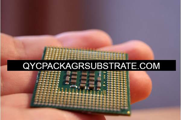
FCCSP Flip Chip CSP Substrate Manufacturer. High speed and high frequency material packaging substrate manufacturing. Advanced packaging substrate production process and technology.
Enter Flip Chip Chip Scale Package (FCCSP), a disruptor in the semiconductor realm with its cutting-edge packaging technology. It flips the script on traditional integrated circuit (IC) packaging by literally flipping the microchip and directly attaching it to the substrate or circuit board. No more bonding pads facing skyward – in flip chip packaging, they gracefully face downward.
Unveiling the standout features of FCCSP:
Chic Compactness: FCCSP brings a chic and compact aesthetic to the table, fitting seamlessly into applications where spatial considerations are paramount.
Snappy Interconnections: Thanks to the direct chip-to-substrate attachment, those interconnections (think copper bumps) get a trim, promoting snappier electrical performance and minimizing pesky signal delays.
Heat Harmony: The direct attachment method not only showcases style but also plays a role in thermal harmony, allowing heat to waltz away more efficiently through the substrate.
Electrical Elevation: Shorter interconnections and a reduction in parasitic capacitance and inductance form a tag team that elevates the electrical performance to new heights.
Density Drama: Flip chip packaging takes center stage in enabling the drama of high-density IC integration on a substrate, laying the groundwork for the creation of intricate and robust electronic marvels.
Versatility Vibes: FCCSP exudes versatility, finding its groove across a vast spectrum of electronic gadgets – from the essentials like mobile phones to the trendsetting digital cameras and beyond.
In essence, FCCSP emerges as a packaging virtuoso, seamlessly blending style, performance, and thermal finesse. It’s not just a choice; it’s the avant-garde selection for a myriad of semiconductor applications.
What is the Manufacturing Process of FCCSP?
The fabrication journey of Flip Chip Chip Scale Package (FCCSP) traverses multiple intricate steps, orchestrating the transformation of a silicon wafer into a sophisticated semiconductor device. While nuances may vary among manufacturers, here’s a broad overview of the FCCSP manufacturing process:
Wafer Prowess:
Commencing with a silicon wafer, this foundational substrate undergoes a metamorphosis through successive depositions of conductive and insulating layers via techniques like chemical vapor deposition (CVD) and physical vapor deposition (PVD).
Circuit Ballet:
The wafer, now a canvas, becomes a stage for the choreography of integrated circuit creation. Photolithography, etching, and doping take center stage, sculpting the circuitry, transistors, and essential components.
Flip Chip Choreography:
Enter the flip chip bonding act. Individual chips pirouette to showcase their active side adorned with bonding pads facing downward. Solder bumps or copper pillars, crafted through methods like electroplating, step onto the stage.
Under Bump Metallization (UBM) Intricacy:
A touch of Under Bump Metallization magic enhances the connection between solder bumps and bonding pads, a metallurgical waltz that ensures reliability and performance.
Substrate Canvas:
The substrate, often a laminate or organic canvas, receives its preparation. Pads or lands emerge, ready to tango with the solder bumps. Layers of traces and vias are woven into the substrate for seamless interconnections.
Flip Chip Assembly Ballet:
The orchestrated dance of precision unfolds as flip-chipped ICs gracefully align with the substrate. A symphony of heat in the reflow furnace transforms solder bumps into secure connections, sealing the partnership.
Encapsulation and Packaging Grandeur:
The grand finale sees the assembled flip chip package adorned with an encapsulating garment, shielding it from environmental elements and mechanical duress. Additional layers may be added for thermal dissipation and electrical insulation.
Testing Symphony:
The curtain rises on the testing symphony. Electrical and thermal tests take center stage, ensuring the performance, functionality, and reliability of the FCCSP.
Final Inspection and Packaging Encore:
The FCCSP, having passed the rigorous tests, takes a bow in the final inspection spotlight before being elegantly packaged for its debut in the technological realm.
In this intricate dance of technology, each step contributes to the creation of FCCSP, a masterpiece in semiconductor packaging.
What are the Different Types of Flip Chip CSP?
Enter the realm of Flip Chip Chip Scale Packages (FCCSPs), a diverse ensemble of configurations finely tuned to cater to an array of applications and specifications. Here’s a tour of some distinctive types:
Flip Chip Ball Grid Array (FCBGA):
FCBGA orchestrates the placement of the flip-chipped IC on a substrate adorned with an array of solder balls, forming the vital connectivity link between the chip and the substrate.
Flip Chip Quad Flat Package (FCQFP):
FCQFP takes center stage with a flip-chipped IC gracefully nested on a substrate boasting a quad flat package outline. The visual aesthetic often adopts a square or rectangular form with a flat demeanor.
Flip Chip Chip on Board (FCCOB):
FCCOB skips the intermediary substrate, as the flip-chipped IC boldly takes its place directly on the circuit board. This type finds favor in applications where spatial efficiency steals the spotlight.
Flip Chip Ball Grid Array Package on Package (FCBGA PoP):
FCBGA PoP introduces a layering spectacle, stacking multiple flip-chipped packages to create a visually captivating package-on-package configuration. A common act in the theatrical realm of space-conscious mobile devices.
Flip Chip Dual In-Line Package (FCDIP):
FCDIP embraces a dual in-line package choreography, featuring pins on two sides for the elegance of through-hole mounting, offering a flexible installation dance.
Flip Chip Land Grid Array (FCLGA):
FCLGA, a kindred spirit to FCBGA, swaps solder balls for an array of lands, intricately woven into the substrate. This array serves as the canvas for the flip-chipped IC attachment.
Flip Chip Small Outline Package (FCSOP):
FCSOP, the maestro of compactness, dons a small outline, making it the virtuoso in applications with stringent space constraints, particularly in the realm of portable electronic devices.
Flip Chip Chip on Flex (FCCoF):
FCCoF embraces flexibility, with the flip-chipped IC gracefully attaching itself to a flexible substrate. A dance of adaptability, catering to applications where flexibility is the leading note.
Flip Chip Ball Grid Array on Flex (FCBGA on Flex):
FCBGA on Flex merges the finesse of flip-chip technology with the flexibility of a pliable substrate, offering a harmonious solution for applications demanding both flexibility and high-density integration.
Flip Chip Package-on-Package (FC PoP):
FC PoP steals the show by stacking multiple flip-chipped packages in a vertical spectacle, creating a compact configuration that delivers heightened functionality and density.
In this diverse symphony of FCCSPs, the stage is set for tailored solutions, where spatial dynamics, electrical performance, and application nuances converge to create a captivating performance in the realm of semiconductor devices.
How Does FCCSP Relate to PCB?
The relationship between Flip Chip Chip Scale Package (FCCSP) and Printed Circuit Board (PCB) is pivotal in the intricate dance of electronic systems. Here’s a nuanced exploration of their connection:
Symbiotic Mounting:
FCCSP, as a packaging marvel, finds its home by directly mounting the microchip onto the substrate or PCB. The PCB, in this symbiotic relationship, becomes the canvas on which the electronic performance unfolds.
Interconnection Ballet:
The solder bumps on the flip-chipped IC engage in a graceful dance, making direct contact with the corresponding pads or lands on the PCB. These interconnections form the intricate pathways that orchestrate the symphony of electronic signals.
Spatial Harmony:
FCCSP, celebrated for its compact form, seamlessly integrates into the limited spaces of the PCB. The direct attachment allows for an efficient spatial choreography, contributing to the harmonious design of electronic systems.
Swift Signal Expressions:
The concise interconnection lengths characteristic of FCCSP contribute to a reduction in signal delays. This swift expressiveness is particularly valuable in applications where precise signal timing is paramount.
Thermal Pas de Deux:
The direct liaison of FCCSP with the PCB extends to thermal dynamics. Heat generated by the IC gracefully dissipates through the PCB, creating a thermal pas de deux that enhances overall performance.
Design Symphony for PCB:
PCB designers partake in a design symphony where the nuances of FCCSP integration are considered. Attention is given to the arrangement of solder bumps, ensuring alignment with PCB pads, and meticulous consideration of thermal factors.
Versatile Integration:
FCCSP seamlessly integrates into the fabric of electronic devices where PCBs play a central role. From mobile phones to cameras, this integration paves the way for the creation of compact and potent electronic wonders.
Flexibility in Substrate Harmony:
FCCSP’s embrace extends to different PCB substrates, from traditional rigid boards to the flexibility of PCBs. This flexibility in substrate choice adds a versatile note to the design palette.
In essence, the dance of FCCSP and PCB unfolds as a harmonious collaboration, where mounting, interconnecting, and integrating form a choreography that defines the elegance and efficiency of electronic systems.
What are the Applications of FCCSP in the Electronics Field?
In the expansive realm of electronics, the Flip Chip Chip Scale Package (FCCSP) emerges as a versatile maestro, orchestrating a symphony of technological advancements across various applications. Let’s embark on a renewed exploration, appreciating the intricate dance of FCCSP in the following domains:
Smartphones – Engineering Elegance:
FCCSP takes center stage in the engineering ballet of smartphones, seamlessly integrating complex circuits within a sleek and compact design. Its efficiency in space utilization adds a touch of elegance to modern mobile devices.
Digital Cameras – Precision Imaging Poetry:
Within the poetry of precision imaging, FCCSP lends its artistry to digital cameras. High-density integration becomes the brushstroke that paints efficient and space-conscious designs in the canvas of photography.
Wearable Devices – Fashioning Innovation:
Wearable electronics, adorned with innovation, find a muse in FCCSP. Its petite dimensions and lightweight charm become the runway for wearable wonders, where technology and personal style converge.
Consumer Electronics – Power in the Palm:
FCCSP commands attention in the realm of consumer electronics, empowering portable audio players and gaming devices. The compact footprint and high-performance capabilities redefine the dynamics of portable electronic powerhouses.
Automotive Electronics – Driving Technological Evolution:
In the driving seat of technological evolution within vehicles, FCCSP finds its place in electronic control units (ECUs) and critical automotive components. Reliability and space efficiency become the fuel for innovation on the roads.
Medical Devices – Healing with Precision:
Medical devices, with a precision mandate, find an ally in FCCSP. It becomes the conduit for smaller and more agile medical electronics, contributing to the evolution of precision healthcare technology.
Networking Equipment – Connectivity Rhapsody:
The connectivity rhapsody in networking devices, embodied by routers and switches, echoes with the high-density integration of FCCSP. This harmony redefines the symphony of connectivity, enhancing the efficiency of networking equipment.
IoT Devices – Nurturing the Digital Ecosystem:
FCCSP becomes a nurturing force in the digital ecosystem of Internet of Things (IoT) devices. Its petite stature packs a technological punch, fostering the integration of diverse functionalities within the compact confines of IoT applications.
Industrial Electronics – Compact Robust Solutions:
Industrial electronics find a reliable companion in FCCSP for electronic components and control systems. The marriage of high-density integration and robust design becomes the blueprint for compact industrial electronic solutions.
Aerospace and Defense – Technological Sentinel in the Skies:
In the vast skies, FCCSP stands as a technological sentinel for aerospace and defense applications. Avionics, communication systems, and critical electronic components soar with reliability and performance.
Smart Sensors – Sensory Innovations:
Smart sensors, pioneers in sensory innovations for IoT and automation, embrace the technological finesse of FCCSP. It becomes the catalyst for sensing the future, encapsulating advanced functionalities within a sensory landscape.
Embedded Systems – Harmony of Size and Intelligence:
In the symphony of embedded systems, where size harmonizes with intelligence, FCCSP emerges as the preferred conductor for integrated circuits. Its technological orchestration resonates in the intricacies of embedded applications.
In this dynamic narrative of electronics, FCCSP plays a versatile role, adding layers of innovation, elegance, and efficiency across a diverse spectrum of applications.
What is the Main Structure and Advanced Manufacturing Technologies of FCCSP?
Unveiling the sophisticated symphony of Flip Chip Chip Scale Packages (FCCSPs) unveils a realm of intricacy where structure and manufacturing technologies converge. Let’s embark on a renewed exploration, delving into the core structure and the choreography of advanced manufacturing:
Structure Ensemble:
Substrate Canvas:
The foundational canvas, known as the substrate, sets the stage. Crafted from materials like silicon or organic laminate, it provides a robust foundation for the ensuing electronic spectacle.
Semiconductor Maestro – Die/Chip:
The semiconductor maestro, the die or chip, takes the spotlight. In a flip-chip ballet, it elegantly flips and bonds, establishing an intimate connection with the substrate, active side down.
Conductive Choreography – Interconnects:
Conductive interconnects perform a delicate dance, forming intricate pathways between the chip and substrate. Solder bumps or metallic pillars lead this choreography, creating direct electrical connections with finesse.
Guardian Veil – Passivation Layer:
A passivation layer emerges as the guardian veil, shielding the chip from environmental elements. Its protective cloak ensures longevity and resilience against moisture and contaminants.
Supporting Artistry – Underfill Material:
Underfill material steps onto the stage, providing support and filling the gaps. This material not only enhances thermal conductivity but also weaves a narrative of mechanical fortitude.
Final Embrace – Encapsulation/Molding Compound:
The final act unfolds with an encapsulation or molding compound, wrapping the entire assembly in a protective embrace. This compound becomes the armor, fortifying the FCCSP against external forces.
Manufacturing Choreography:
Wafer Prelude:
The manufacturing journey commences with the wafer prelude. Semiconductor wafers undergo a series of transformative processes, including photolithography, etching, and deposition, setting the stage for individual semiconductor devices.
Flip-Chip Ballet:
The flip-chip ballet takes center stage, orchestrated with precision. The chip, in a graceful inversion, bonds directly to the substrate. Automated equipment conducts this dance, ensuring alignment and connection perfection.
Underfill Symphony:
Following the flip-chip spectacle, the underfill symphony commences. Material is delicately dispensed around solder bumps, filling voids. The curing process solidifies this symphony, ensuring thermal and adhesive excellence.
Encapsulation/Molding Extravaganza:
An encapsulation or molding extravaganza ensues, using avant-garde materials. This artistic process molds the FCCSP into its final form, providing durability and resilience against environmental forces.
Testing Sonata:
A testing sonata echoes through the manufacturing stage. Electrical, thermal, and visual inspections harmonize to validate the FCCSP’s functionality and quality, ensuring a flawless performance.
Material Alchemy:
The alchemy of materials unfolds, incorporating high-performance solder alloys, thermally efficient underfill compounds, and cutting-edge encapsulation materials. This material alchemy weaves a tale of reliability and superior performance.
Dimensional Symphony – 3D Packaging:
The dimensional symphony takes shape with 3D packaging technologies. Stacking configurations like Package-on-Package or vertically integrating components adds a layer of innovation to the manufacturing narrative.
Wafer-Level Artistry:
Wafer-level packaging unveils an artistry where multiple chips are embraced simultaneously. This streamlined approach at the wafer level introduces efficiency and elevates cost-effectiveness.
Fine Pitch Elegance:
Fine pitch technologies add an element of elegance, allowing for closely spaced solder bumps. This precision ensures accommodation of an extensive network of connections within a confined space.
Metrology Marvels:
Advanced metrology and inspection tools emerge as marvels, ensuring the precision and quality of manufacturing processes. Optical inspections, X-ray examinations, and non-destructive testing methods contribute to structural integrity.
In this symphony of materials and processes, FCCSPs emerge not just as electronic components but as a manifestation of the seamless fusion of artistry and technology. Each solder bump, substrate, and encapsulation compound plays a role in creating compact, high-performance masterpieces.
Frequently Asked Questions (FAQs)
What does FCCSP stand for?
FCCSP stands for Flip Chip Chip Scale Package.
How does FCCSP differ from other packaging technologies?
FCCSP distinguishes itself by directly attaching the flipped chip to the substrate, leading to a compact form factor and high-density integration compared to other packaging technologies.
What are the advantages of using FCCSP?
Advantages encompass a compact size, high-density integration, minimized signal delays, efficient thermal performance, and suitability for space-constrained applications.
Who are the key manufacturers of FCCSP?
Key manufacturers include semiconductor packaging and electronic component specialists with expertise in advanced packaging technologies.
How does FCCSP contribute to miniaturization in electronic devices?
FCCSP contributes to miniaturization by enabling direct chip attachment, reducing the overall footprint of integrated circuits, and supporting the design of compact and portable electronic devices.
What is the significance of fine pitch technologies in FCCSP?
Fine pitch technologies facilitate closely spaced solder bumps or interconnects, allowing for a higher density of connections, a critical factor in accommodating numerous connections within confined spaces.
Are there different types of FCCSP configurations?
Yes, FCCSP configurations can vary based on specific application requirements. Additionally, 3D packaging technologies may be employed for more intricate configurations.
Conclusion
In summary, Flip Chip Chip Scale Packages (FCCSPs) represent a pinnacle of technological sophistication and packaging ingenuity. This avant-garde packaging technique, marked by the direct fusion of semiconductor chips with substrates, has heralded a paradigm shift towards compactness and heightened integration in the realm of electronic devices.
The intricate ensemble of FCCSP components, including substrates, semiconductor chips, interconnects, underfill materials, passivation layers, and encapsulation compounds, orchestrates a symphony of precision and utility. This condensed structure not only optimizes spatial efficiency but also elevates thermal performance, positioning FCCSP as a preferred choice across diverse industries.
The manufacturing odyssey of FCCSP unfolds as a choreographed sequence of refined processes. From the graceful dance of flip-chip bonding to the meticulous dispensing and curing of underfill materials, each step contributes to the crafting of resilient and dependable electronic packages. Advanced technologies, such as wafer-level packaging, fine pitch configurations, and the dimensionality introduced by 3D packaging, inject layers of complexity and innovation into the manufacturing narrative.
FCCSP’s application canvas spans a wide spectrum, gracing smartphones, digital cameras, wearables, automotive systems, medical devices, and beyond. Its pivotal role in driving the miniaturization of electronic devices is irrefutable, presenting a solution perfectly aligned with the contemporary demand for sleek and portable designs.
As we navigate the landscape of electronic packaging, FCCSP emerges not just as a utilitarian solution but as a transformative catalyst. The perpetual evolution of manufacturing technologies and the embrace of fine pitch configurations underscore its adaptability and enduring relevance in a dynamic technological milieu. In essence, FCCSP transcends its role as a packaging solution, embodying a force that shapes our interaction with electronic devices—forging a future that is not just smaller but smarter, more efficient, and inherently connected.