
FCCSP Package Substrate Manufacturer.High speed and high frequency material packaging substrate manufacturing. Advanced packaging substrate production process and technology.
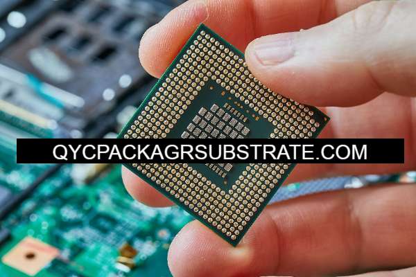
BT FCCSP Package Substrate, which stands for Ball Terminal Flip Chip Chip Scale Package Substrate, represents a paradigm shift in packaging solutions dedicated specifically to integrated circuits (ICs). By artfully integrating ball-shaped terminals and adopting a flip chip design within a compact substrate, this technology has firmly positioned itself as a linchpin in the realm of high-performance and densely configured IC assemblies.
The distinctive attributes of the FCCSP Package Substrate lie in its remarkable density, superior performance, and a conspicuously compact physical footprint. The incorporation of ball terminals and the ingenious flip chip architecture not only facilitates an increased number of connection points within confined spaces but also enhances the operational efficiency and overall functionality of integrated circuits. Furthermore, the strategic use of chip-scale package substrates ensures an aesthetically pleasing, streamlined packaging design, contributing to the development of sleek, lightweight devices.
The versatility of the BT FCCSP Package Substrate spans across diverse industries, including mobile devices, communication equipment, and automotive electronics. In these arenas, where the demand for reduced dimensions, heightened performance, and enhanced reliability takes center stage, the FCCSP Package Substrate emerges as an indispensable solution. This advanced packaging technology serves as a catalyst for innovation in the electronics industry, charting the course for the creation of next-generation smart devices seamlessly combining power, compactness, and portability.
What are the Functions of FCCSP Package Substrate?
The BT FCCSP Package Substrate assumes a pivotal role in shaping the landscape of integrated circuits (ICs) and cutting-edge packaging technology, encompassing a spectrum of essential functions:
Conduit for Electrical Signals: At its core, the substrate acts as a conduit, orchestrating seamless electrical connectivity between the integrated circuit (IC) and external components or the printed circuit board (PCB). This is achieved through the innovative integration of ball-shaped terminals and a flip chip design, ensuring the efficient flow of electrical signals.
Optimization of Space: A standout feature lies in the substrate’s ability to accommodate a high density of connection points within a confined space. This characteristic is instrumental in fostering intricate IC designs, enabling not only miniaturization but also an augmentation of overall electronic device performance.
Thermal Harmony: The substrate contributes significantly to the thermal equilibrium of the IC by facilitating effective heat dissipation. This aspect is critical in preventing overheating and underpins the reliable functionality of high-performance integrated circuits.
Guardian of Mechanical Integrity: Beyond its electrical role, the substrate functions as a stalwart guardian, providing essential mechanical support and shielding the delicate IC components from physical stress and environmental elements.
Streamlined Aesthetics: The chip-scale design of the substrate doesn’t just serve a functional purpose; it contributes to the aesthetic sleekness of device designs. This is particularly salient in applications where size and weight constraints are decisive factors, such as in the design of mobile devices and wearable technology.
Elevated Electrical Performance: The advanced architecture of BT FCCSP translates into an elevation of electrical performance, minimizing signal interference, and augmenting the overall functionality of integrated circuits.
Harmony with Advanced Technologies: Engineered with foresight, the substrate seamlessly integrates with state-of-the-art semiconductor manufacturing processes. This ensures compatibility with advanced technologies and materials, underscoring its role in optimizing performance.
Reliability Bastion: Serving as a reliable foundation, the BT FCCSP Package Substrate enhances the overall reliability of IC packaging. This becomes paramount in applications where electronic components face diverse environmental conditions and mechanical stresses.
In essence, the BT FCCSP Package Substrate emerges as a multifaceted linchpin, not merely facilitating electrical connections but shaping the very fabric of IC packaging. Its contributions span from enhancing performance and miniaturization to effective thermal management, encapsulating the essence of reliability in electronic devices.
What are the Different Types of FCCSP Package Substrate?
Within the domain of FCCSP (Ball Terminal Flip Chip Chip Scale Package) Substrates, a rich tapestry of potential variations unfolds, each crafted to cater to nuanced demands in the ever-evolving landscape of semiconductor packaging. While the specifics of individual types may be subject to the dynamic pace of technological progress, overarching characteristics and potential distinctions offer insight:
Artistry in Ball Terminal Designs:
The realm of ball terminal design presents an array of possibilities, encompassing variations in size, shape, and material composition. These subtleties wield influence over the intricate dance of electrical and thermal performance.
Palette of Substrate Materials:
The canvas of substrate materials is broad, spanning from traditional organic substrates to avant-garde options like ceramics. This selection acts as a palette, where each material choice contributes to the brushstrokes of crucial aspects such as thermal conductivity, reliability, and cost-effectiveness.
Dimensions and Form Factor Symphony:
BT FCCSP Substrates orchestrate a symphony of sizes and form factors, harmonizing with the diverse dimensions of integrated circuits. This symphony is finely tuned to meet the bespoke requirements of varied applications.
Alignment with Technology Choreography:
Each variant of BT FCCSP substrate partakes in a dance with technology generations, aligning itself with the latest choreography of manufacturing processes and materials that define the rhythmic progression of semiconductor packaging.
Integration Ballet with Advanced Technologies:
Some substrates elegantly engage in a ballet of integration with advanced technologies. This dance may involve partnering with innovative interconnect solutions, participating in avant-garde packaging techniques, or gracefully embracing the three-dimensional dynamics of integration methods.
Tailored Variations for Special Performances:
Tailored performances take the stage, with substrates designed to meet the unique demands of specific applications. These bespoke renditions may include specialized substrates curated for high-frequency overtures, the automotive electronics ensemble, or those destined for high-power crescendos.
How Does FCCSP Package Substrate Differ from PCB?
In the intricate realm of electronic systems, the FCCSP (Ball Terminal Flip Chip Chip Scale Package) substrate and the ubiquitous Printed Circuit Board (PCB) play distinctive roles, each lending its unique characteristics to the orchestration of electronic functionalities. Here, we delineate the discernible differences between the BT FCCSP Package Substrate and PCB:
Designated Purpose:
BT FCCSP Package Substrate: Positioned as a specialized platform exclusively tailored for the mounting and connection of flip-chip integrated circuits (ICs), excelling in scenarios where stringent demands for space efficiency and high performance prevail.
PCB: Assumes the versatile role of a foundational canvas, accommodating a myriad of electronic components, including resistors, capacitors, and ICs, catering to a broad spectrum of applications.
Attachment Techniques Choreography:
BFCCSP Package Substrate: Orchestrates a performance centered around flip-chip IC attachment, where the IC elegantly flips, and its bond pads forge direct connections with the substrate via solder balls, optimizing for compactness and efficiency.
PCB: Conducts a diverse symphony of component attachment techniques, from surface mounting to through-hole components, allowing for an expressive range of possibilities in electronic design.
Integration Aesthetics:
BT FCCSP Package Substrate: Showcases its prowess in high-density integration, sculpting a compact form with a myriad of connection points—an artistry perfectly suited for applications that demand the finesse of miniaturization.
PCB: Boasts flexibility in size and complexity, a canvas adaptable to the artistic visions of designers, scalable to meet the demands of applications ranging from the elegantly simple to the intricately complex.
Manufacturing Ballet:
FCCSP Package Substrate: Takes center stage with its choreography of advanced packaging technologies, where flip-chip assembly requires precision in execution to achieve a seamless dance of reliable electrical connections.
PCB: Participates in a standard manufacturing pas de deux, involving processes such as copper layer etching onto a substrate. It can be a single-sided, double-sided, or multi-layered performance, depending on the complexity of the composition.
Application Spotlight:
FCCSP Package Substrate: Illuminated in applications where the spotlight falls on the trifecta of space, weight, and performance, such as in the graceful performance of mobile devices, wearables, and high-performance computing ensembles.
PCB: Casts its versatile glow across diverse stages, finding a role in computers, communication devices, automotive systems, and more, showcasing adaptability to a multitude of settings.
Artistry of Design Versatility:
BT FCCSP Package Substrate: Crafts its performance with a keen focus on high-density IC packaging, a masterpiece fine-tuned for a specific set of functionalities.
PCB: Paints a tapestry of versatility, allowing for the artistic expression of diverse electronic components, providing a canvas for the realization of various design visions.
In essence, the BT FCCSP Package Substrate and PCB, though both luminaries in the electronic ensemble, perform distinct movements in the grand symphony of electronic design—offering specialized prowess in high-density IC packaging and providing a versatile stage for an array of electronic components, respectively.
What are the Key Structures and Manufacturing Technologies of BT FCCSP Package Substrate?
Harmony of Key Structures:
Substrate Material Ballet:
The very essence lies in the substrate material, a fundamental choice ranging from sophisticated ceramics to the versatile embrace of organic laminates. This selection crafts the backdrop, influencing thermal conductivity, electrical attributes, and the overall tapestry of reliability.
Ball Terminal Choreography:
BT FCCSP showcases a choreography of ball terminals, strategically poised for the electrical pas de deux between the integrated circuit (IC) and the substrate. These spherical performers, carefully arranged, compose a visual and functional symphony in the pursuit of a compact design.
Flip Chip Elegance:
The heart of the performance is the flip chip configuration, an elegant inversion where the IC gracefully reveals its active side. Direct connection to the substrate is orchestrated through solder balls, a dance that optimizes electrical prowess and interconnection density.
Die Attach Artistry:
The securing act unfolds with die attach materials—adhesives or solders—crafted to ensure a secure and mechanically stable connection. This act, performed with precision, forms the foundation for the subsequent movements.
Underfill Melody:
A subtle melody resonates with the use of underfill material, filling the spaces between the IC and the substrate. This composition not only offers mechanical support but also harmonizes with the strains of reliability, addressing thermal cycling and mechanical stresses.
Intricacies of Manufacturing Technologies:
Flip Chip Assembly Symphony:
The core of the manufacturing stage is the flip chip assembly, a grand symphony where the flipped IC delicately partners with the substrate using solder bumps or balls. Precision in alignment takes center stage, ensuring the flawless union of IC bond pads with their substrate counterparts.
Ball Attach Ballet:
The ball attach process follows suit, securing the ball terminals to the substrate through an array of techniques, from soldering to advanced bonding. This ballet of attachment adds layers of complexity to the manufacturing performance.
Solder Mask and Layer Crescendo:
As the substrate evolves, a crescendo is reached with processes like solder mask application and layer buildup. These steps, dictated by design nuances, contribute to the package’s reliability and functionality, forming a dynamic movement in the overall composition.
Testing and Inspection Drama:
The drama unfolds in rigorous testing and inspection procedures—electrical tests, meticulous visual inspections, and a suite of quality control measures that stand as guardians, ensuring the integrity of each BT FCCSP package.
Equipment Ensemble:
The manufacturing stage is set with an ensemble of advanced equipment—automated pick-and-place maestros, soldering virtuosos, and precision inspection instruments—all harmonizing to achieve the desired level of precision and consistency.
As the saga of semiconductor packaging continues to evolve, seeking the latest insights entails delving into the specifications provided by semiconductor manufacturers or consulting authoritative industry publications. The BT FCCSP Package Substrate, with its intricate structures and manufacturing technologies, emerges as a testament to the artistry and innovation propelling the realm of advanced electronic packaging.
Frequently Asked Questions (FAQs)
What Defines BT FCCSP Package Substrate?
BT FCCSP (Ball Terminal Flip Chip Chip Scale Package) Substrate serves as a specialized platform for semiconductor packaging, enabling the connection of flip-chip integrated circuits (ICs) with ball-shaped terminals, fostering compact and high-density designs.
Who Leads in Manufacturing BT FCCSP Package Substrates?
Industry frontrunners in BT FCCSP Package Substrate manufacturing include Amkor Technology, ASE Group, STATS ChipPAC, and other eminent semiconductor packaging entities renowned for their prowess in advanced packaging technologies.
Which Materials Take Center Stage in BT FCCSP Substrate Production?
The materials employed in BT FCCSP Substrate manufacturing span from organic laminates to advanced ceramics. This material choice intricately shapes thermal conductivity, electrical properties, and overall reliability.
How Does BT FCCSP Stand Out Among Packaging Technologies?
BT FCCSP distinguishes itself through a flip-chip configuration, orchestrating the inversion of the IC and establishing direct connections between bond pads and the substrate using solder balls. This design excels in high-density integration for space-constrained applications.
What Advantages Does BT FCCSP Package Substrate Offer?
Key advantages encompass high integration density, efficient thermal management, and a streamlined form factor. Its prowess is particularly showcased in applications demanding miniaturization, including mobile devices, wearables, and high-performance computing.
Can BT FCCSP Substrates Thrive in High-Frequency Environments?
With appropriate design considerations, BT FCCSP substrates can be tailored to support high-frequency applications. Manufacturers may offer specialized variants optimized for specific performance criteria.
Unveiling the Manufacturing Process of BT FCCSP Substrates:
The manufacturing journey involves a symphony of processes—flip chip assembly, ball attachment, solder mask application, layer buildup, and meticulous testing. Advanced equipment, including automated pick-and-place machines, ensures a ballet of precision and consistency.
Is Customization Available for BT FCCSP Substrates in Specific Applications?
Absolutely. Manufacturers extend customization options to align with the unique demands of diverse applications. This may involve tailored substrate materials, sizes, and configurations to harmonize with the requirements of the end-use device.
What Measures Ensure Quality in BT FCCSP Substrate Production?
Rigorous quality control measures encompass electrical testing, visual inspections, and strict adherence to industry standards. Manufacturers adhere to stringent processes to guarantee the reliability and performance of BT FCCSP packages.
Where Can I Access Technical Specifications for BT FCCSP Package Substrates?
Technical specifications are readily available on the official websites of BT FCCSP substrate manufacturers. Additionally, industry publications and technical documents offer comprehensive insights into the specifications and capabilities of these substrates.
Conclusion
In conclusion, the world of BT FCCSP (Ball Terminal Flip Chip Chip Scale Package) substrates unveils a fascinating realm of innovation and precision within semiconductor packaging. As we navigate this landscape, key manufacturers such as Amkor Technology, ASE Group, and STATS ChipPAC stand as pioneers, orchestrating a symphony of advanced packaging technologies.
The essence of BT FCCSP lies in its role as a specialized platform, seamlessly integrating flip-chip ICs with ball-shaped terminals to achieve compact and high-density designs. The choice of substrate materials, whether organic laminates or advanced ceramics, adds nuance to the performance, shaping thermal conductivity, electrical attributes, and overall reliability.
This packaging technology distinguishes itself through a graceful flip-chip configuration, perfectly suited for high-density integration in applications where space is a premium. The advantages it brings to the stage—high integration density, efficient thermal management, and a sleek form factor—make it a star performer in the realm of miniaturization, gracing applications like mobile devices, wearables, and high-performance computing.
As we delve into the intricacies of manufacturing, the process unfolds like a choreographed ballet—flip chip assembly, ball attachment, solder mask application, layer buildup—all meticulously executed with advanced equipment to ensure precision and consistency.
Customization takes center stage, offering tailored experiences for diverse applications. Manufacturers craft bespoke solutions, adjusting substrate materials, sizes, and configurations to harmonize with the unique demands of end-use devices.
Quality control measures, akin to a performance prelude, become the guardian of reliability. Rigorous testing, visual inspections, and adherence to industry standards ensure that each BT FCCSP package takes its place as a reliable and high-performing component in electronic systems.
The technical symphony, with its detailed specifications and capabilities, is readily accessible on the official websites of manufacturers. Industry publications and technical documents contribute to a comprehensive repertoire, offering insights into the evolving landscape of BT FCCSP package substrates.
In essence, the conclusion of this exploration leaves us with an appreciation for the intricate dance of technology, where BT FCCSP substrates play a vital role, seamlessly blending innovation, customization, and reliability in the ever-evolving field of semiconductor packaging.