
Flip Chip Chip Scale Package Substrates Manufacturer
Flip Chip Chip Scale Package Substrates Manufacturer,Flip Chip Chip Scale Package (FCCSP) substrates are advanced interconnection platforms used in semiconductor packaging. They facilitate the direct attachment of a silicon die to the substrate via solder bumps, which are flipped over and bonded, hence the term “flip chip.” These substrates are typically composed of high-performance materials like BT resin or organic laminates, providing excellent electrical and thermal characteristics. FCCSP substrates enable higher input/output (I/O) density, improved electrical performance, and better thermal management compared to traditional wire bonding techniques. Their compact size and efficient design make them ideal for applications in high-speed computing, mobile devices, and other miniaturized electronic products.
What is Flip Chip Chip Scale Package Substrates?
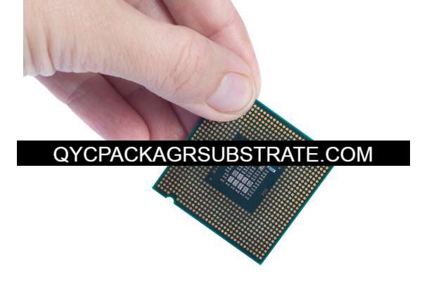
Flip Chip Chip Scale Package (FCCSP) substrates are a type of advanced packaging technology used in semiconductor manufacturing. They provide a platform for mounting and interconnecting semiconductor chips, allowing for direct electrical connection between the chip’s bumps and the substrate pads. Unlike traditional wire-bonding methods, flip chip technology involves flipping the chip so that its active side faces down, enabling a more compact and efficient design.
FCCSP substrates are characterized by their small size and high-density interconnects, making them ideal for applications where space is at a premium. They are commonly used in smartphones, tablets, wearable devices, and other compact electronic products. The flip chip design helps to reduce the overall footprint of the package, enhance signal integrity, and improve thermal performance.
The substrates themselves are made from materials such as organic laminates, ceramics, or other advanced materials that offer excellent electrical and thermal properties. They are designed to support high-speed and high-frequency applications, making them suitable for use in cutting-edge technologies like 5G communications, advanced computing, and high-performance graphics.
The FCCSP technology allows for the integration of multiple functions within a single package, enabling the development of more powerful and efficient electronic devices. This packaging method supports various types of chips, including processors, memory, and specialized components, making it a versatile solution for modern electronics.
Flip Chip Chip Scale Package Substrates Manufacturer
What are the Flip Chip Chip Scale Package Substrates Design Guidelines?
Designing Flip Chip Chip Scale Package (FCCSP) substrates involves several critical guidelines to ensure optimal performance and reliability. Here are key considerations:
- Substrate Material Selection: Choose materials that offer excellent thermal and electrical properties. Common materials include organic laminates, ceramics, and advanced polymers. The material should also support high-density interconnections and offer good thermal dissipation.
- Bump Design: Design the bumps (solder or conductive) with appropriate size and pitch to ensure reliable electrical connections. Bump spacing and alignment are crucial to achieving a high-density interconnect layout.
- Thermal Management: Incorporate adequate heat dissipation features to manage the thermal load generated by the chip. This may involve using heat sinks, thermal vias, or specific materials with high thermal conductivity.
- Electrical Performance: Ensure that the substrate design supports high-speed signal transmission and minimizes signal loss and crosstalk. This involves optimizing trace routing, impedance control, and maintaining signal integrity.
- Mechanical Strength: The substrate should be designed to withstand mechanical stresses during assembly and operation. This includes considering the coefficient of thermal expansion (CTE) to match the chip and substrate materials.
- Design for Manufacturability: Ensure that the design allows for reliable and efficient manufacturing processes. This includes considerations for alignment accuracy, soldering processes, and quality control.
- Testing and Reliability: Design the substrate to facilitate testing and ensure long-term reliability. This involves incorporating test pads and ensuring that the design can withstand various environmental conditions, such as temperature fluctuations and mechanical stresses.
- Compliance with Standards: Follow industry standards and guidelines, such as IPC standards, to ensure compatibility and quality. Adhering to these standards helps in achieving consistency and reliability across different manufacturing processes.
By adhering to these guidelines, you can design FCCSP substrates that provide high performance, reliability, and manufacturability, meeting the demanding requirements of modern electronic applications.
What is the Flip Chip Chip Scale Package Substrates Fabrication Process?
The fabrication process for Flip Chip Chip Scale Package (FCCSP) substrates involves several key steps to ensure the precise manufacturing of high-performance substrates. Here’s an overview of the typical fabrication process:
- Substrate Material Preparation: Begin with selecting and preparing the substrate material, which could be an organic laminate, ceramic, or advanced polymer. The material is processed into thin, flat sheets or layers, which will form the base of the package.
- Photoresist Coating: Apply a layer of photoresist material to the substrate. This material will be used to define the circuit patterns on the substrate. The photoresist is then baked to harden it and make it ready for patterning.
- Patterning: Use photolithography to expose the photoresist to light through a mask. The mask defines the circuit patterns and bump pads. After exposure, develop the photoresist to create a pattern that reveals areas of the substrate for etching.
- Etching: Etch the substrate to remove unwanted material and create the necessary circuit paths and pads. This step is crucial for forming the electrical connections and features on the substrate.
- Deposition: Deposit metal layers onto the substrate to form electrical traces and pads. Commonly used metals include copper, gold, and silver. Techniques like sputtering or electroplating may be used to apply these metal layers.
- Via Formation: Create vias, or vertical connections, in the substrate. This involves drilling or etching holes through the substrate and then filling them with metal to form electrical connections between different layers of the substrate.
- Bump Formation: Apply solder bumps or conductive bumps to the designated pads on the substrate. These bumps will later connect to the chip’s bond pads. Techniques like electroplating or stencil printing are commonly used for bump formation.
- Die Attachment: Attach the semiconductor die (chip) to the substrate. The die is flipped and aligned so that its bumps make contact with the substrate’s pads. Soldering or adhesive bonding is used to secure the die.
- Encapsulation: Encapsulate the assembly to protect it from environmental factors. This can involve using a molding compound or other protective materials to cover the die and bumps.
- Testing and Inspection: Perform thorough testing and inspection to ensure the quality and functionality of the FCCSP. This includes checking for electrical connections, mechanical integrity, and adherence to design specifications.
- Dicing and Packaging: Cut the substrate into individual packages, ensuring that each FCCSP meets the required specifications. Final packaging involves placing the substrates into their respective protective and transport packaging.
By following these fabrication steps, manufacturers can produce high-quality FCCSP substrates that meet the demanding requirements of modern electronics, providing reliable performance and efficient integration for various applications.
How Do You Manufacture Flip Chip Chip Scale Package Substrates?
Manufacturing Flip Chip Chip Scale Package (FCCSP) substrates involves several intricate steps to ensure high precision and reliability. Here’s a detailed overview of the manufacturing process:
- Material Selection and Preparation: Choose appropriate substrate materials, such as organic laminates (e.g., FR-4, BT), ceramics, or advanced polymers. Prepare the material by cutting it into thin, flat sheets or panels that will serve as the base for the substrate.
- Photoresist Application: Apply a photoresist layer onto the prepared substrate. This layer is used to define the circuit patterns. The photoresist is then baked to harden it and make it ready for patterning.
- Photolithography and Patterning: Expose the photoresist-coated substrate to ultraviolet (UV) light through a photomask that defines the circuit patterns. Develop the photoresist to create a patterned layer that reveals areas for etching and metal deposition.
- Etching: Etch the exposed substrate areas to remove unwanted material and form the necessary circuit traces and pads. This can involve both wet and dry etching techniques, depending on the substrate material and design requirements.
- Metal Deposition: Deposit metal layers onto the substrate to form electrical traces, pads, and other conductive features. Techniques such as sputtering, electroplating, or chemical vapor deposition (CVD) are used to apply metals like copper, gold, or silver.
- Via Formation: Create vias (vertical electrical connections) by drilling or etching holes through the substrate layers. Fill these vias with metal to ensure electrical connectivity between different layers of the substrate.
- Bump Formation: Apply solder or conductive bumps to the designated pads on the substrate. Bump formation is achieved through methods like stencil printing, electroplating, or bumping machines. These bumps will later interface with the chip’s bond pads.
- Die Bonding: Attach the semiconductor die to the substrate. The die is aligned and flipped so that its bumps make contact with the substrate’s pads. This process involves solder reflow or adhesive bonding to securely attach the die.
- Encapsulation: Protect the die and bumps by encapsulating the assembly with a molding compound or protective resin. This step ensures durability and shields the internal components from environmental damage.
- Curing and Hardening: Cure or harden the encapsulation material as required, which may involve heating or chemical processes to achieve the desired physical properties.
- Testing and Inspection: Perform extensive testing and inspection to verify the functionality, electrical performance, and mechanical integrity of the FCCSP substrates. This includes checking for proper connections, verifying electrical characteristics, and ensuring compliance with design specifications.
- Dicing and Final Packaging:Cut the substrate into individual FCCSP units using precision dicing equipment. Package the finished substrates to protect them during handling and shipping.
By following these manufacturing steps, high-quality FCCSP substrates are produced, ensuring reliable performance and integration in a wide range of electronic applications.
How Much Should Flip Chip Chip Scale Package Substrates Cost?
The cost of Flip Chip Chip Scale Package (FCCSP) substrates can vary widely based on several factors. Here’s a breakdown of the elements that influence the cost:
- Material: The choice of substrate material—whether it’s an organic laminate, ceramic, or advanced polymer—affects the cost. High-performance or specialized materials typically increase the overall cost.
- Design Complexity: The complexity of the substrate design, including the number of layers, the density of interconnections, and the bump pattern, impacts the cost. More intricate designs require advanced fabrication processes, which can drive up the price.
- Size and Thickness: Larger or thicker substrates generally cost more due to the increased material usage and processing requirements.
- Volume: Economies of scale play a significant role in cost. Higher production volumes usually result in lower per-unit costs due to reduced manufacturing and setup expenses.
- Bump Specifications: The type and size of the bumps, as well as their placement and alignment precision, can affect the cost. Specialized bumping techniques or materials can increase the cost.
- Lead Time: Expedited or rush orders may incur additional costs. Standard lead times are typically more cost-effective.
- Quality and Reliability Requirements: Substrates designed for high-reliability applications or those that require stringent testing and inspection may have higher costs due to the additional quality assurance measures.
- Manufacturing Technology: The use of advanced manufacturing technologies, such as high-precision photolithography, metal deposition, or advanced encapsulation techniques, can also influence the cost.
In general, the cost of FCCSP substrates can range from a few dollars to several tens of dollars per unit, depending on the factors mentioned. For specific pricing, it is best to consult with manufacturers or suppliers who can provide quotes based on the exact requirements and quantities needed.
What is Flip Chip Chip Scale Package Substrates Base Material?
The base material for Flip Chip Chip Scale Package (FCCSP) substrates plays a crucial role in determining the substrate’s performance characteristics, such as electrical, thermal, and mechanical properties. The choice of base material affects the overall reliability and functionality of the package. Here are the commonly used base materials:
- Organic Laminates: These are the most widely used materials for FCCSP substrates due to their versatility and cost-effectiveness. They typically consist of a composite of epoxy resins and glass fibers, such as FR-4 or BT (bismaleimide-triazine) resins. Organic laminates offer good electrical insulation, ease of processing, and are suitable for a wide range of applications.
- Ceramics: Ceramic materials, such as alumina (Al₂O₃) or aluminum nitride (AlN), are used in FCCSP substrates for applications requiring high thermal conductivity and electrical performance. Ceramics provide excellent heat dissipation and electrical insulation, making them ideal for high-performance and high-frequency applications.
- Advanced Polymers: Materials like polyimide and liquid crystal polymers (LCP) are used for their high-temperature stability and low dielectric constants. These advanced polymers are often selected for their ability to handle high-speed and high-frequency signals.
- Epoxy-Glass Composites: These composites are used for their mechanical strength and thermal stability. They are often used in conjunction with other materials to provide a balance of performance characteristics.
- High-Density Interconnect (HDI) Materials: In some advanced FCCSP designs, HDI materials are used to support high-density interconnections and fine-pitch bump patterns. These materials often involve a combination of organic and ceramic components to meet specific design requirements.
The choice of base material depends on the specific requirements of the FCCSP, including thermal management, electrical performance, and mechanical durability. Each material type offers different advantages and is selected based on the intended application and performance criteria.
Which Company Makes Flip Chip Chip Scale Package Substrates?
There are many companies in the market that manufacture Flip Chip Chip Scale Package (FCCSP) substrates, including Intel, TSMC, Samsung Electronics, Qualcomm, and Taiwan Semiconductor Manufacturing Company (TSMC). These companies have advanced technology and equipment in the field of FCCSP substrate manufacturing, producing high-performance FCCSP substrates that are widely used in smartphones, tablets, high-performance computing, and other applications.
Intel is renowned for its advanced semiconductor packaging technology, and its FCCSP substrates offer excellent electrical performance and thermal management capabilities. TSMC has rich experience in high-density interconnects and high-performance applications for FCCSP substrates, with its products widely used in high-end electronic products. Samsung Electronics is known for its innovative packaging solutions, providing high integration and high reliability in FCCSP substrates. Qualcomm and TSMC also have deep technical expertise in FCCSP substrate manufacturing and R&D, meeting the demands of various high-requirement applications.
Our company also has the capability to manufacture FCCSP substrates. Our FCCSP substrates use high-performance base materials to ensure excellent performance in high-density interconnect and high-frequency applications. Our FCCSP substrate products have the following features:
- High-Performance Materials: We use high-quality base materials, such as high thermal conductivity and high-frequency materials, to ensure stability and low loss of the substrate under high-density interconnect conditions.
- Precision Processing: Our company has advanced processing equipment and a skilled technical team to achieve high-precision circuit processing and packaging, ensuring high-quality products.
- High Integration Design: We can design and manufacture high-integration FCCSP substrates based on customer requirements to meet the needs of complex circuits and high-performance applications.
- Comprehensive After-Sales Service: We provide comprehensive after-sales service to ensure that customers receive timely technical support and solutions during use.
- Customized Service: We offer customized FCCSP substrate design and manufacturing services according to specific customer needs, ensuring that the products fully meet the application requirements.
Through continuous technological innovation and strict quality control, our FCCSP substrates have gained widespread recognition in the market and are widely used in smartphones, computers, and other high-performance electronic devices. If you have FCCSP substrate needs, please contact us, and we will provide you with high-quality products and services.
In summary, whether it is from material selection, processing technology, or after-sales service, our company has the capability to produce high-quality FCCSP substrates to meet the needs of various high-performance applications.
What are the 7 Qualities of Good Customer Service?
Good customer service is crucial for building strong relationships with customers and ensuring their satisfaction. Here are seven key qualities of excellent customer service:
- Empathy: Understanding and sharing the feelings of customers helps in addressing their concerns effectively. Empathy involves actively listening to customers, acknowledging their emotions, and showing genuine care for their issues.
- Responsiveness: Timely and efficient responses to customer inquiries and issues are essential. Being prompt in addressing questions or problems demonstrates respect for the customer’s time and helps in resolving issues quickly.
- Knowledgeable Staff: Having well-trained and knowledgeable staff ensures that customers receive accurate and helpful information. Staff should be familiar with products, services, and company policies to provide reliable support.
- Clear Communication: Effective communication involves being clear, concise, and transparent. Using simple language and avoiding jargon helps customers understand information easily, and keeping them informed about the status of their requests or issues is important.
- Patience: Patience is vital when dealing with frustrated or confused customers. Providing a calm and supportive response, even in challenging situations, helps in resolving issues and maintaining a positive customer experience.
- Problem-Solving Skills: Good customer service requires the ability to identify and resolve problems efficiently. This involves thinking critically, offering practical solutions, and taking ownership of issues until they are resolved to the customer’s satisfaction.
- Positive Attitude: A friendly and positive attitude can make a significant difference in customer interactions. Being courteous, respectful, and enthusiastic helps create a welcoming atmosphere and leaves a lasting impression on customers.
By incorporating these qualities into customer service practices, businesses can enhance customer satisfaction, build loyalty, and create a positive reputation.
FAQs about Flip Chip Chip Scale Package Substrates
What is a Flip Chip Chip Scale Package (FCCSP) substrate?
An FCCSP substrate is a type of semiconductor packaging that allows for high-density interconnections between the chip and the package. It involves placing a semiconductor die directly on the substrate with solder bumps, minimizing the package size and improving performance.
What materials are commonly used for FCCSP substrates?
Common materials include organic laminates (such as FR-4 and BT), ceramics, and advanced polymers. Each material has specific benefits in terms of thermal conductivity, electrical performance, and mechanical properties.
What industries use FCCSP substrates?
FCCSP substrates are widely used in industries such as consumer electronics, telecommunications, automotive, and high-performance computing. They are found in devices like smartphones, tablets, and computer processors.
How are FCCSP substrates manufactured?
The manufacturing process involves material preparation, photoresist application, photolithography, etching, metal deposition, bump formation, die attachment, encapsulation, and final testing. These steps ensure the substrate meets performance and reliability standards.
What are the typical applications of FCCSP substrates?
FCCSP substrates are used in applications requiring high-density interconnections and compact packaging, such as mobile phones, tablets, and high-speed processors.
What are the challenges in using FCCSP substrates?
Challenges include managing thermal dissipation, ensuring precise alignment of the die and bumps, and achieving high manufacturing yields. These factors are crucial for maintaining the performance and reliability of the final product.