
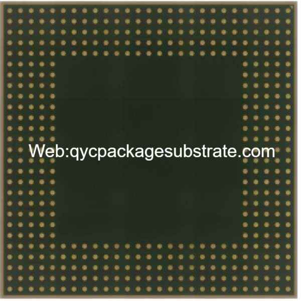
Flip Chip CSP (FCCSP) Manufacturer. we can produce the best samllest bump pitch with 100um, the best smallest trace are 9um. and the smallest gap are 9um. most of the design are 15um to 30um trace and spacing.
Flip Chip Chip Scale Package (Flip Chip CSP) emerges as a revolutionary packaging solution in the dynamic realm of semiconductors, tailor-made for integrated circuits (ICs). Let’s unravel the nuances of these terms:
Flip Chip: Breaking away from the conventional tether of wire bonding to attach the semiconductor die to a package substrate, flip chip technology introduces a paradigm flip. The semiconductor die is inverted, and its active facet, adorned with electrical connections or bumps, establishes a direct connection with the package substrate or an alternative carrier through solder bumps. This departure paves the way for abbreviated interconnection paths, heightened electrical prowess, and superior heat dissipation.
Chip Scale Package (CSP): CSP emerges as a distinct breed of IC packaging meticulously crafted to mirror, in nearly identical dimensions, the size of the enclosed semiconductor die. The primary objective is to shrink the package footprint, achieving the pinnacle of compactness. CSPs find application in scenarios demanding spatial efficiency, weight reduction, and heightened thermal performance in electronic devices.
In essence, Flip Chip CSP seamlessly amalgamates the virtues of flip chip technology with the spatial optimization finesse of chip scale packaging. The resulting advantages span enhanced electrical efficiency, a sleek physical profile, and superior thermal regulation—positioning it as a discerning choice for applications where spatial considerations, epitomized in mobile devices and compact electronic gadgets, take precedence.
What are the Key Functions of FCCSP?
The Flip Chip Chip Scale Package (FCCSP) serves as a multifaceted powerhouse, executing crucial functions within the intricate landscape of semiconductor packaging. Let’s unravel the distinctive roles it plays:
Sleek Design for Space Maximization: FCCSP is intricately crafted to emulate the dimensions of the enclosed semiconductor die, championing spatial efficiency. This streamlined design proves indispensable in scenarios where spatial constraints demand meticulous consideration.
Optimized Electrical Dynamics: Leveraging the ingenuity of flip chip technology, FCCSP strategically shortens the interconnection paths between the semiconductor die and the package substrate. This optimization translates into a surge in electrical performance, minimizing signal delays, and elevating the overall functionality of the integrated circuit.
Efficient Thermal Dissipation: The direct fusion of the flip-chipped semiconductor die with the package substrate facilitates seamless heat dissipation. This plays a pivotal role in sustaining optimal operating temperatures, ensuring the robustness and endurance of the integrated circuit.
Trimmed Weight and Agile Form Factor: Through a calculated design approach and the omission of certain packaging components, FCCSP contributes to an overall reduction in weight. This feature holds particular significance in applications where weight considerations wield considerable influence, such as in portable electronic devices.
Championing Miniaturization: FCCSP empowers the miniaturization of electronic devices by delivering a packaging solution intricately aligned with the dimensions of the semiconductor die. This capability proves instrumental in sculpting smaller, more nimble gadgets.
Amplified Connectivity: The utilization of solder bumps for direct connections amplifies connectivity between the semiconductor die and the package substrate. This enhancement in connectivity translates into superior signal integrity and seamless data transfer within the integrated circuit.
In essence, FCCSP stands as a versatile virtuoso, excelling in spatial efficiency, electrical optimization, thermal finesse, weight reduction, miniaturization, and enhanced connectivity. Collectively, these attributes position FCCSP as a dynamic and influential force across a spectrum of semiconductor applications.
What are the Different Types of Flip Chip CSP?
Within the expansive realm of Flip Chip Chip Scale Packages (CSPs), a myriad of types unfurls, each weaving its distinctive tapestry of characteristics and applications. Here’s a glimpse into the diverse variations:
Copper Pillar Flip Chip CSP (Cu Pillar FC-CSP): This type gracefully adopts copper pillars as the electrical connection bumps, fostering a seamless link between the semiconductor die and the package substrate. Revered for their superior electrical and thermal performance, copper pillars take center stage.
Solder Bump Flip Chip CSP (Solder Bump FC-CSP): A stalwart choice, this variant relies on solder bumps for electrical connections. While lacking the avant-garde allure of copper pillars, solder bumps persist as a pervasive and reliable solution.
Non-Conductive Paste Flip Chip CSP (NC Paste FC-CSP): Departing from the norm of metal bumps, this type embraces non-conductive paste for connections. Esteemed for its cost-effectiveness, it finds a niche in applications where precision at a fine pitch is paramount.
Gold Bump Flip Chip CSP (Au Bump FC-CSP): Gold bumps claim the spotlight for electrical connections in this type. Offering impeccable conductivity, the use of gold may, however, entail a higher cost compared to alternative materials.
Fan-Out Wafer-Level Package (FO-WLP): While not strictly adhering to the conventional flip chip CSP archetype, FO-WLP stands out by redistributing connections across a broader area on the package substrate. This opens the door to an expanded array of input/output connections.
Embedded Wafer-Level Ball Grid Array (eWLB): Drawing parallels with FO-WLP, eWLB redistributes connections to the package substrate but elevates the game by embedding the entire semiconductor die within the package, fortifying it for enhanced protection.
These diverse incarnations of Flip Chip CSPs respond to specific needs—whether it be the pursuit of heightened electrical performance, judicious cost considerations, or application-specific requisites. The choice among these types pivots on factors like the intended application, sought-after performance benchmarks, and financial considerations.
How do FCCSP Manufacturers Contribute to IC Packaging?
Enterprises specialized in crafting Flip Chip Chip Scale Packages (FCCSP) wield significant influence, steering the evolution of integrated circuit (IC) packaging within the semiconductor industry. Their diverse contributions span various dimensions, introducing innovations and refinements. Here’s an in-depth exploration of how FCCSP manufacturers actively shape the landscape of IC packaging:
Innovative Design Frontier: Situated at the forefront of innovation, FCCSP manufacturers consistently explore and implement cutting-edge designs. Their commitment to pioneering designs not only amplifies the electrical performance and thermal regulation of ICs but also elevates the overall functional capabilities.
Strategic R&D in Material Science: These manufacturers make substantial investments in research and development, particularly in materials used in FCCSP. This involves the exploration and experimentation of diverse bump materials (such as copper, solder, or non-conductive paste) and substrate materials, all aimed at enhancing reliability, durability, and overall performance.
Championing Miniaturization Initiatives: Acknowledged for its compact form, FCCSP serves as a catalyst behind the ongoing miniaturization of electronic devices. Manufacturers actively refine processes that enable miniaturization, paving the way for the creation of smaller yet more potent ICs across diverse applications.
Continuous Advancements in Manufacturing Techniques: FCCSP manufacturers relentlessly refine and optimize manufacturing processes. Progress in flip chip assembly, bumping techniques, and overall production methodologies is continually explored to enhance production efficiency and mitigate costs.
Tailored Solutions for Varied Applications: Recognizing the diverse needs across industries, manufacturers offer bespoke solutions. This includes tailoring bump materials, adjusting package sizes, and configuring setups to align precisely with specific requirements spanning consumer electronics to automotive systems.
Meticulous Quality Control Practices: Ensuring the dependability of IC packages is a top priority. FCCSP manufacturers implement stringent quality control measures and rigorous reliability testing, aligning with industry standards. Comprehensive testing covers aspects such as thermal performance, mechanical stress, and overall durability.
Fostering Collaboration within the Ecosystem: FCCSP manufacturers actively engage in collaborative efforts with other stakeholders in the semiconductor ecosystem. Partnerships extend to semiconductor design firms, testing and assembly companies, and end-users, fostering seamless integration of FCCSPs into the broader semiconductor supply chain.
Embracing Environmental Sustainability: A discernible shift towards environmentally conscious packaging solutions is evident. FCCSP manufacturers explore materials and processes aligned with sustainability goals and global environmental standards, embodying a commitment to responsible practices.
In essence, FCCSP manufacturers emerge as architects of change, propelling innovation in design, materials, and manufacturing practices. Their contributions extend beyond technical excellence, encompassing customization, quality assurance, collaborative endeavors, and a steadfast commitment to environmental responsibility, collectively shaping the trajectory of IC packaging technology.
What are the Differences Between FCCSP and Traditional PCBs?
Flip Chip Chip Scale Packages (FCCSP) and traditional Printed Circuit Boards (PCBs) inhabit distinct niches within the electronic landscape, each boasting unique architectures and functionalities. Let’s navigate through the core distinctions that set FCCSP apart from traditional PCBs:
Packaging Precision:
FCCSP: Precision is the hallmark of FCCSP packaging, tailored explicitly for integrated circuits. Utilizing flip chip technology, it orchestrates a direct attachment of the chip to the package substrate, fostering an ethos of spatial efficiency.
Traditional PCB: In contrast, traditional PCBs serve as the canvas for electronic components without embodying a specific packaging type. They provide a foundational platform for elements like integrated circuits, resistors, capacitors, and connectors.
Connection Dynamics:
FCCSP: The connectivity in FCCSP unfolds through flip chip bonding, a nuanced process involving the flipping of the chip and its direct connection to the package substrate using solder bumps or alternative conductive materials.
Traditional PCB: Components on a traditional PCB adhere to conventional soldering methods, diverging from the direct flip chip bonding characteristic intrinsic to FCCSP.
Dimensions and Design Philosophy:
FCCSP: Engineered with a keen eye on miniaturization, FCCSP embodies a compact form factor intricately aligned with the dimensions of the semiconductor die. It excels in applications where spatial constraints reign supreme.
Traditional PCB: Traditional PCBs, in contrast, exhibit versatility in size and shape, with dimensions dictated by the overarching requirements of the electronic system they underpin.
Applications Spectrum:
FCCSP: FCCSP stakes its claim in applications demanding miniaturization, high-density packaging, and superior electrical performance. Its prowess finds expression in realms such as mobile devices, wearables, and other compact electronic marvels.
Traditional PCB: Traditional PCBs epitomize versatility, finding utility across a spectrum ranging from modest consumer gadgets to intricate systems like computers and industrial machinery.
Integration Prowess:
FCCSP: A trailblazer in integration, FCCSP seamlessly embeds the semiconductor die into the package. This integration prowess translates into heightened electrical performance and reduced signal delays.
Traditional PCB: While flexible in amalgamating diverse components, traditional PCBs fall short of achieving the same level of integration witnessed in FCCSP.
Manufacturing Odyssey:
FCCSP: The manufacturing journey of FCCSP involves the precision of flip chip bonding—meticulously aligning and affixing the chip to the substrate. Advanced methodologies, including copper pillar bumping, may come into play.
Traditional PCB: Traditional PCBs traverse well-trodden manufacturing paths, featuring established processes like etching, drilling, and soldering. Flip chip bonding remains outside the conventional purview.
In essence, FCCSP and traditional PCBs are denizens of different realms. FCCSP takes the lead in arenas clamoring for miniaturization, high-density packaging, and direct chip integration, while traditional PCBs thrive as versatile canvases accommodating a diverse array of electronic elements. The choice unfolds based on the specific imperatives of the application at hand.
What is the Main Structure and Production Technology of FCCSP?
Unlocking the mysteries of the Flip Chip Chip Scale Package (FCCSP) reveals a captivating blend of complexity in structure and a meticulously choreographed production journey. Let’s embark on a journey to unveil the intricate components shaping the FCCSP structure and unravel the nuances of its production technology:
Symphony of FCCSP Architecture:
Semiconductor Core:
The FCCSP narrative unfolds with the semiconductor die taking center stage, acting as the core orchestrator of the electronic symphony within the device.
Substrate Canvas:
Providing a robust canvas, the substrate sets the stage for the semiconductor die, facilitating an elegant performance of electrical connections.
Bump Harmonies:
Bumps, crafted from materials like solder or copper, play the role of conductors, harmonizing the efficient transmission of signals between the semiconductor die and the substrate.
Underfill Ballet:
A ballet of structural resilience ensues with the application of underfill material, delicately dispensed to fill the spaces between the semiconductor die and the substrate. This choreography ensures grace amidst thermal expansion challenges.
Passivation Shield:
A passivation layer emerges as a protective shield, guarding the semiconductor die against external elements such as moisture, contaminants, and the unpredictable nature of the performance.
Encapsulation Aura:
The ensemble enters an encapsulating aura, as a protective layer—often crafted from epoxy molding compound (EMC)—encases the entire performance. This encapsulation stands as a guardian, shielding the components from the crescendos of the environment and mechanical stresses.
Ballet of FCCSP Production:
Wafer Overture:
The overture begins with the artistry of wafer processing, a symphony of processes like photolithography, etching, and deposition that crafts semiconductor wafers, setting the stage for the performance.
Bumping Choreography:
Bumping takes center stage in a choreographed dance, delicately adding bumps to the contact pads on the semiconductor die. These bumps set the stage for the intricate dance of flip chip bonding.
Flip Chip Bonding Pas de Deux:
In a pas de deux of precision, the semiconductor die executes a flip, engaging in a meticulous dance with the substrate. Bumps on the die and corresponding pads on the substrate come together in a dance of direct contact, orchestrated with finesse through controlled heating for a secure and reliable bond.
Underfill Crescendo:
The crescendo of underfill material follows, dispensed with precision around the periphery of the flip-chip assembly. This material, akin to a crescendo, flows beneath the semiconductor die, elevating structural support and reliability.
Curing and Encapsulation Ensemble:
The ensemble of curing solidifies the underfill material, and the entire performance is encapsulated with a protective layer, often featuring the harmonious notes of epoxy molding compound (EMC). This encapsulation stands as an ensemble, shielding the components from the external symphony.
Testing Sonata:
The sonata of testing ensues, a meticulous composition validating electrical harmony, structural integrity, and the overall symphony of reliability. Tests encompass a melodic array of electrical assessments, thermal cycling harmonies, and visual inspections that resonate with precision.
Trim and Form Finale:
The grand finale involves a delicate trim of excess material and a graceful form, preparing the FCCSP for its entrance into electronic devices with a touch of elegance.
The production ballet of FCCSP unfolds with precision, finesse, and a symphony of materials, yielding a compact, high-performance package. This intricate dance caters to applications where spatial constraints and optimal electrical performance take center stage.
Frequently Asked Questions (FAQs)
What are the primary benefits of opting for FCCSP?
FCCSP offers a range of advantages, including a compact size, high integration density, reduced interconnection lengths, improved electrical performance, and suitability for applications with stringent space constraints.
Which industries commonly leverage FCCSP technology?
FCCSP finds widespread usage in industries such as consumer electronics (e.g., smartphones, wearables), automotive electronics, medical devices, and other sectors where achieving miniaturization and high performance is critical.
Which materials are typically employed in the manufacturing of FCCSP?
The materials used in FCCSP manufacturing encompass the semiconductor die, substrate materials, bump materials (e.g., solder, copper), underfill materials, passivation layers, and encapsulation materials (e.g., epoxy molding compound).
What is the significance of the bumping process in FCCSP manufacturing?
Bumping holds crucial importance in FCCSP manufacturing as it involves the addition of bumps to the contact pads on the semiconductor die. These bumps play a pivotal role in facilitating the flip chip bonding process and establishing essential electrical connections.
In what ways does FCCSP contribute to advancements in integrated circuit (IC) packaging?
FCCSP contributes significantly by providing a packaging solution that enables higher integration density, superior electrical performance, and a more compact form factor for integrated circuits. This addresses the evolving needs of modern electronic devices requiring efficient and space-saving packaging.
What quality control measures are implemented by FCCSP manufacturers?
FCCSP manufacturers adhere to stringent quality control measures, incorporating electrical testing, thermal cycling tests, visual inspections, and other assessments to ensure the reliability, functionality, and structural integrity of the packaged devices.
Conclusion
In drawing the curtains on our exploration, the narrative of Flip Chip Chip Scale Packages (FCCSP) unfurls as a compelling journey through the intricate realm of semiconductor packaging. This cutting-edge technology, characterized by its intricate structure and exacting production processes, emerges as a linchpin in the narrative of modern electronics. Beyond overcoming spatial constraints, FCCSP stands as a compact and high-performance solution that resonates across diverse applications.
The craftsmen behind FCCSP manufacturing play a pivotal role, conducting a symphony of processes—from wafer processing to bumping, flip chip bonding, encapsulation, and testing. This choreographed tapestry yields a package that not only meets the demands of miniaturization but also excels in delivering optimal electrical performance, seamlessly integrating into the landscapes of consumer electronics and the robust domains of automotive innovation.
As technology propels forward, FCCSP stands as a beacon of innovation, pushing the boundaries of integrated circuit packaging with an adaptability that positions it at the forefront of the dynamic semiconductor landscape.
In summary, FCCSP transcends conventional packaging; it is a manifestation of precision, ingenuity, and an unwavering commitment to meeting the ever-evolving needs of electronic devices. The narrative of FCCSP unfolds as a tale of technological sophistication, where the convergence of form and function shapes the future of electronics with an unmistakable blend of elegance and efficiency.