
Flip Chip Substrates Manufacturer
Flip Chip Substrates Manufacturer,Flip Chip substrates are advanced packaging solutions designed for high-performance electronic devices. They support flip chip technology, where integrated circuits are mounted face-down on the substrate, allowing for direct electrical connections and enhanced signal integrity. These substrates are crafted from high-quality materials that provide excellent thermal conductivity and electrical performance. Flip Chip substrates enable high-density interconnections and reduced signal path lengths, making them ideal for applications requiring compact designs and efficient heat dissipation, such as in processors, memory chips, and high-speed communication systems. Their robust construction ensures reliable operation and durability in demanding environments.
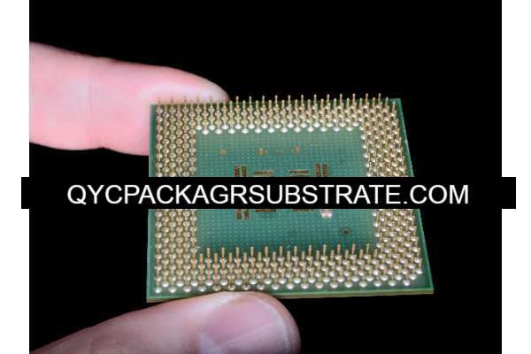
What is a Flip Chip Substrate?
A Flip Chip Substrate is a critical component used in advanced electronic packaging to facilitate high-performance and high-density interconnections between a semiconductor chip and its package. The term “flip chip” refers to the method of mounting the chip onto the substrate. In this approach, the semiconductor chip is flipped upside down and directly bonded to the substrate using solder bumps or balls, which serve as the electrical interconnections.
The Flip Chip Substrate itself is a specialized type of printed circuit board (PCB) or interposer that provides the physical and electrical interface between the chip and the rest of the electronic system. It is designed to handle high-density interconnections, enabling greater performance and miniaturization of electronic devices. These substrates often use advanced materials and techniques to support high-speed data transmission and manage heat dissipation.
Materials commonly used for Flip Chip Substrates include high-frequency laminates, ceramic, or advanced organic materials. They are engineered to accommodate the specific needs of flip chip technology, including high thermal conductivity and low signal loss.
In summary, a Flip Chip Substrate is essential for modern electronics, allowing for the efficient transfer of signals and heat between the semiconductor chip and the external circuitry, thus supporting the performance and reliability of advanced electronic systems.
Flip Chip Substrates Manufacturer
What are the Flip Chip Substrate Design Guidelines?
Designing a Flip Chip Substrate involves several critical guidelines to ensure optimal performance, reliability, and manufacturability. Here are some key considerations:
- Thermal Management: Ensure that the substrate can effectively dissipate heat generated by the chip. Use materials with high thermal conductivity, such as copper or aluminum, and incorporate thermal vias or heat spreaders to enhance heat dissipation.
- Signal Integrity: Maintain signal integrity by minimizing signal loss and crosstalk. Use high-frequency laminates and design the traces with appropriate impedance matching. Keep traces short and use differential pairs for high-speed signals.
- Via Design: Implement vias carefully to avoid signal degradation and thermal issues. Ensure that vias are properly plated and that their size and spacing are optimized to handle the required current and maintain signal integrity.
- Solder Bumps: Design the layout and placement of solder bumps to ensure reliable electrical connections. Ensure that the bump pitch and size match the specifications of the chip and the substrate to avoid bridging and misalignment.
- Mechanical Support: Provide adequate mechanical support to avoid warping or deformation of the substrate during the soldering process. Consider using reinforcement layers or stiffeners if necessary.
- Electrical Isolation: Ensure proper electrical isolation between different layers and components to prevent short circuits and interference. Use appropriate dielectric materials and maintain proper spacing between traces.
- Design for Manufacturability: Design the substrate to be easily manufacturable. This includes ensuring that the layout is within the capabilities of the fabrication process and that the design rules comply with industry standards.
- Testing and Reliability: Incorporate design features that facilitate testing and inspection, such as test pads and inspection marks. Ensure the design supports reliability requirements, including thermal cycling and mechanical stress.
- Compliance with Standards: Adhere to industry standards and guidelines for flip chip substrates, such as IPC standards, to ensure compatibility and reliability in electronic systems.
By following these design guidelines, you can optimize the performance and reliability of Flip Chip Substrates, ensuring they meet the demanding requirements of modern electronic applications.
What is the Flip Chip Substrate Fabrication Process?
The fabrication process for Flip Chip Substrates involves several intricate steps to ensure that the substrate meets the required performance and reliability standards. Here’s an overview of the typical steps involved:
- Material Preparation: Select and prepare the base material for the substrate, which could be a high-frequency laminate, ceramic, or organic material. The choice of material depends on the specific requirements of the flip chip application.
- Layer Deposition: Apply the conductive layers (e.g., copper) onto the substrate material. This is typically done through processes such as sputtering or electroplating. The conductive layers will eventually form the circuit traces and pads.
- Photoresist Application and Patterning: Coat the substrate with a photoresist material, which is sensitive to light. The photoresist is then exposed to ultraviolet (UV) light through a mask that defines the circuit pattern. The exposed areas are developed and removed, leaving behind a patterned photoresist layer that will guide subsequent etching processes.
- Etching: Use chemical etching or plasma etching to remove the unwanted conductive material, leaving behind the desired circuit pattern. This step defines the traces and pads on the substrate.
- Via Formation: Create vias (small holes) in the substrate where electrical connections will be made between different layers. This can be done through drilling or laser ablation. The vias are then plated with metal to ensure conductivity.
- Solder Bump Formation: Apply solder bumps or balls to the pads where the semiconductor chip will be mounted. This is typically done using processes such as solder paste printing and reflow soldering. The size and pitch of the solder bumps are crucial for proper alignment and electrical connection.
- Dielectric Layer Deposition: Deposit dielectric layers between conductive layers to provide electrical insulation. This step may include applying and curing additional layers of insulating materials.
- Final Etching and Cleaning: Perform final etching to remove any residual materials and clean the substrate to prepare it for chip bonding.
- Testing and Inspection: Conduct electrical testing and visual inspection to ensure that the substrate meets design specifications and performance requirements. This step may include checks for connectivity, impedance, and thermal properties.
- Chip Mounting: Flip the semiconductor chip and align it with the solder bumps on the substrate. Use reflow soldering to attach the chip to the substrate, allowing the solder bumps to melt and form electrical connections.
- Final Assembly and Packaging: Complete the assembly process by encapsulating the substrate and chip in a protective package if needed. This may involve additional steps such as molding, encapsulation, and further testing.
Throughout the fabrication process, precision and attention to detail are crucial to ensure that the Flip Chip Substrate performs reliably in its intended application.
How do you Manufacture a Flip Chip Substrate?
The manufacturing of a Flip Chip Substrate involves a series of detailed and precise steps to create a high-performance, reliable interconnection platform for semiconductor chips. Here is a step-by-step overview of the process:
- Material Selection and Preparation: Begin by selecting the appropriate substrate material, which can be a high-frequency laminate, ceramic, or an advanced organic material. Prepare the material by cutting it to the desired size and cleaning it to remove any contaminants.
- Copper Foil Lamination: Laminate thin layers of copper foil onto the substrate material. This copper layer will form the conductive pathways. The lamination process involves applying heat and pressure to bond the copper foil to the substrate.
- Photoresist Coating and Patterning: Apply a photoresist coating to the copper surface. Expose the photoresist to ultraviolet (UV) light through a photomask that contains the pattern of the circuitry. Develop the photoresist to remove the exposed areas, leaving behind a protective pattern on the copper.
- Etching:Perform an etching process to remove the unwanted copper from the areas not protected by the photoresist. This reveals the desired circuitry pattern on the substrate. Etching can be done using chemical or plasma methods.
- Via Drilling and Plating: Drill vias (small holes) in the substrate to create vertical connections between different layers. These vias are then plated with metal (usually copper) to ensure electrical conductivity. The plating process involves filling the vias with a conductive material.
- Dielectric Layer Deposition: Deposit dielectric materials over the copper circuitry to provide electrical insulation between different layers. This may involve applying and curing multiple layers of dielectric material.
- Solder Bump Formation:Apply solder bumps to the pads on the substrate where the semiconductor chip will be mounted. This is typically done using solder paste printing followed by reflow soldering, which melts the solder to form bumps that will make electrical connections with the chip.
- Final Etching and Surface Preparation:Conduct final etching to clean up any residual materials and prepare the surface for chip attachment. This may involve additional cleaning and surface treatments to ensure good adhesion and reliability.
- Testing and Inspection: Perform rigorous testing and inspection to verify that the substrate meets design specifications and performance standards. Tests may include electrical testing, impedance measurements, and visual inspections.
- Chip Bonding: Align and attach the semiconductor chip to the substrate using the solder bumps. This is done by flipping the chip and placing it onto the substrate, then reflowing the solder to create reliable electrical connections.
- Encapsulation and Packaging: Finally, encapsulate the assembled substrate and chip in a protective package if required. This step may include additional processes such as molding, encapsulation, and final assembly to protect the substrate and chip from environmental damage.
By following these steps with precision, manufacturers can produce Flip Chip Substrates that offer high performance, reliability, and durability for advanced electronic applications.
How Much Should a Flip Chip Substrate Cost?
The cost of a Flip Chip Substrate can vary widely based on several factors:
- Material Type:The choice of substrate material (e.g., high-frequency laminate, ceramic, or organic materials) significantly impacts cost. High-frequency materials and ceramics are generally more expensive than standard organic materials.
- Complexity and Design:Substrates with more complex designs, including multiple layers, fine-pitch solder bumps, and intricate via structures, typically cost more due to the increased manufacturing challenges and requirements for precision.
- Size and Dimensions: Larger substrates or those with custom dimensions can be more expensive due to the higher material and processing costs.
- Volume: The cost per unit decreases with higher production volumes due to economies of scale. Prototype or low-volume production can be significantly more expensive per unit than mass production.
- Manufacturing Technology: Advanced fabrication techniques and quality control processes can add to the cost. High-speed, high-density interconnections and advanced materials generally involve more sophisticated technology.
- Additional Features: Special requirements such as enhanced thermal management, high reliability, or specific environmental conditions can increase costs.
- Supplier and Region: Costs can also vary depending on the supplier and region due to differences in labor costs, overhead, and market conditions.
As a rough estimate, the cost of a Flip Chip Substrate can range from a few dollars to several hundred dollars per unit. For basic substrates, costs might start around $10 to $50 per unit, while more complex or specialized substrates can range from $100 to $300 or more per unit.
For accurate pricing, it’s best to consult with substrate manufacturers or suppliers, providing them with detailed specifications and requirements to get a precise quote.
What is Flip Chip Substrate Base Material?
The base material of a Flip Chip Substrate is crucial for ensuring the substrate’s performance, reliability, and compatibility with the chip and the overall electronic system. Here’s an overview of common base materials used for Flip Chip Substrates:
- High-Frequency Laminates: These materials are designed for applications requiring high-speed signal transmission and minimal signal loss. They typically consist of layers of fiber-reinforced epoxy resin or other composite materials. High-frequency laminates, such as those made from PTFE (Polytetrafluoroethylene) or ceramic-filled composites, offer excellent electrical performance and are used in applications like RF (Radio Frequency) and microwave circuits.
- Ceramic Materials: Ceramics, such as alumina (Al2O3) or beryllium oxide (BeO), are used for their high thermal conductivity and electrical insulation properties. Ceramic substrates are often employed in high-power or high-reliability applications due to their robustness and ability to handle significant thermal and mechanical stresses.
- Organic Laminates: These are commonly used for Flip Chip Substrates and include materials like FR-4 (Flame Retardant 4), polyimide, or other epoxy-based composites. Organic laminates are suitable for a wide range of applications due to their cost-effectiveness and good electrical and mechanical properties.
- Metal Core Materials: Some Flip Chip Substrates use metal core materials, such as copper or aluminum, for enhanced thermal management. These substrates feature a metal core layer sandwiched between dielectric layers to efficiently dissipate heat generated by the chip.
- Flexible Materials: For applications requiring flexibility or conformability, flexible substrates made from materials like polyimide or PET (Polyethylene Terephthalate) may be used. These materials are suitable for flexible electronics or applications where the substrate needs to conform to irregular shapes.
- Hybrid Materials: In some advanced applications, a combination of different materials may be used to achieve the desired electrical, thermal, and mechanical properties. Hybrid substrates may incorporate layers of organic laminates, ceramics, and metal cores.
Each base material is selected based on the specific requirements of the application, including electrical performance, thermal management, mechanical strength, and cost considerations. The choice of base material significantly influences the overall performance and reliability of the Flip Chip Substrate in its intended use.
Which Company Makes Flip Chip Substrates?
Many companies manufacture Flip Chip Substrates, including several prominent ones:
- Foxconn: As a global leader in electronics manufacturing services, Foxconn has extensive experience in Flip Chip Substrates. The company utilizes Flip Chip technology in high-end electronic products, offering high-performance substrate solutions.
- Hitachi Chemical: Hitachi Chemical has a long history in electronic materials and substrate manufacturing. They provide various high-performance Flip Chip Substrates, particularly excelling in high-frequency and high-density applications.
- Corning: Corning, a leading high-tech materials supplier, offers advanced ceramic and glass substrates for various electronic applications, including Flip Chip Substrates.
- Xilinx: As a leader in FPGA and programmable logic devices, Xilinx also manufactures Flip Chip Substrates used in its products, especially for high-performance computing and communication applications.
- China Electronics Technology Group Corporation (CETC): In China, CETC is a major electronics manufacturer providing a range of electronic substrate solutions, including Flip Chip Substrates, widely used in defense and communication fields.
Our company also manufactures Flip Chip Substrates. We are dedicated to providing high-quality Flip Chip substrate solutions suitable for various advanced electronic applications. Our company has advanced manufacturing facilities and technology, capable of supporting the production of high-density, high-performance Flip Chip Substrates, meeting diverse customer needs.
We cover the entire production process, from material selection and design optimization to final production and testing, ensuring that each Flip Chip Substrate meets the highest quality standards and performance requirements.
We emphasize customized services based on customer needs, whether for small-batch prototypes or large-scale production, offering flexible solutions. Our engineering team works closely with clients to ensure that every detail in the design and manufacturing process meets their specifications and requirements.
If you are interested in our Flip Chip Substrate manufacturing capabilities, please feel free to contact us for detailed technical support and quotation information.
What Are the 7 Qualities of Good Customer Service?
Good customer service is essential for building strong relationships with customers and fostering loyalty. Here are seven key qualities of excellent customer service:
- Responsiveness:Quick and effective responses to customer inquiries and issues are crucial. Good customer service involves addressing customer concerns promptly, whether through phone, email, or chat, and ensuring that customers feel heard and valued.
- Empathy:Understanding and relating to the customer’s situation is important. Empathetic customer service representatives listen actively, show genuine concern, and provide solutions that reflect an understanding of the customer’s feelings and needs.
- Knowledgeability: Customer service representatives should have in-depth knowledge about the products or services they are supporting. This expertise allows them to provide accurate information, solve problems effectively, and offer valuable advice to customers.
- Patience: Dealing with customers requires patience, especially when they are frustrated or confused. A patient representative remains calm, gives customers the time they need, and avoids rushing or interrupting them.
- Communication Skills: Clear and effective communication is key. This includes speaking clearly, using positive language, and ensuring that information is conveyed in a way that the customer can easily understand. Good communication also involves listening carefully and asking clarifying questions when necessary.
- Reliability: Customers need to trust that their issues will be resolved as promised. Reliable customer service means following through on commitments, providing consistent support, and ensuring that solutions are implemented as agreed.
- Courtesy: Politeness and professionalism should be evident in all customer interactions. Courteous service includes using polite language, addressing customers respectfully, and maintaining a positive attitude even in challenging situations.
These qualities collectively contribute to creating a positive customer experience, enhancing satisfaction, and building long-term loyalty.
FAQs
What is the difference between a flip chip substrate and a traditional PCB?
Flip chip substrates are designed specifically for high-density interconnection and performance, while traditional PCBs are generally used for less demanding applications.
How do I choose the right flip chip substrate for my application?
Consider factors such as electrical performance, thermal management, mechanical support, and material properties specific to your application’s requirements.
Can flip chip substrates be used for high-frequency applications?
Yes, flip chip substrates can be designed to handle high-frequency signals, but it’s important to select appropriate materials and design features to ensure performance.
What is the lead time for manufacturing flip chip substrates?
Lead time can vary depending on the complexity of the design and the manufacturer’s capacity. It’s best to consult with the manufacturer for specific time estimates.
How do I ensure the quality of flip chip substrates?
Work with reputable manufacturers, and ensure thorough testing and quality control processes are in place.