
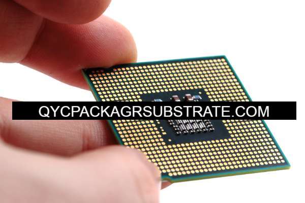
Genclad Materials PCB Manufacturer
Genclad Materials PCB Manufacturer,Genclad Materials PCB is an advanced printed circuit board substrate known for its exceptional performance in high-frequency and high-speed applications. It features a unique laminate construction with enhanced dielectric properties, providing low signal loss and stable electrical characteristics across a broad frequency range. Genclad Materials PCBs are engineered for reliability and durability in demanding environments such as telecommunications, aerospace, and automotive electronics. They support intricate circuit designs and miniaturization, facilitating efficient signal transmission and ensuring superior connectivity. Genclad Materials PCBs are preferred for their robustness and capability to meet stringent performance requirements in modern electronic systems requiring high-speed data transmission and reliable operation.
What is Genclad Materials PCB?
Genclad Materials PCB refers to a type of printed circuit board (PCB) that incorporates materials produced by Genclad Materials Corporation. These PCBs are designed to meet specific performance criteria in electronic applications. Genclad Materials is known for providing advanced materials that enhance the performance and reliability of PCBs, particularly in demanding environments where factors like heat dissipation, signal integrity, and mechanical strength are crucial.
These materials typically include advanced laminates, substrates, and coatings that are engineered to provide superior electrical properties, thermal management capabilities, and resistance to environmental factors such as moisture and corrosion. Genclad Materials PCBs are often used in high-frequency applications, telecommunications, aerospace, automotive electronics, and other industries requiring high reliability and performance from their electronic systems.
The expansion of Genclad Materials PCBs to meet the needs of applications up to 300 words might include details on specific product lines, their unique features such as impedance control, low loss tangent, or high thermal conductivity, and how they contribute to the overall efficiency and longevity of electronic devices. These PCBs are a testament to ongoing advancements in materials science applied to electronics manufacturing, supporting innovations in technology across various sectors globally.
Genclad Materials PCB Manufacturer
What are the Genclad Materials PCB Design Guidelines?
Genclad Materials provides specific design guidelines for PCBs to ensure optimal performance and reliability. These guidelines are crucial for engineers and designers aiming to leverage Genclad materials effectively in their circuit board designs. While the exact details may vary based on the specific materials and applications, here are some general aspects typically covered in Genclad Materials PCB design guidelines:
- Material Selection: Guidelines often include recommendations for selecting the appropriate Genclad materials based on the application requirements. This involves considerations such as dielectric constant, thermal conductivity, coefficient of thermal expansion (CTE), and mechanical strength.
- Layer Stackup Design: Instructions on how to design the layer stackup to achieve desired impedance control, signal integrity, and thermal management. This includes specifying the thickness and order of layers for optimal performance.
- Impedance Control: Guidelines for maintaining consistent impedance throughout the PCB traces, which is critical for high-frequency applications to ensure signal integrity and minimize losses. This may involve specifying trace width, spacing, and layer thicknesses.
- Thermal Management: Recommendations for managing heat dissipation within the PCB, especially important for materials with enhanced thermal conductivity. This could include placing thermal vias strategically, optimizing copper pour, and considering heatsinks or thermal pads.
- Manufacturing Tolerances: Information on manufacturing tolerances and design rules that ensure manufacturability while maintaining performance characteristics. This might involve minimum trace widths, spacing between features, and clearance requirements.
- Mechanical Considerations:Guidelines related to mechanical stability and reliability, including recommendations on board thickness, drill sizes, and reinforcement techniques.
- Environmental Factors: Considerations for environmental durability, such as resistance to moisture, chemicals, and temperature variations. Guidelines may include recommendations for conformal coating or other protective measures.
- Testing and Validation:Suggestions for testing and validating the PCB design to ensure it meets performance specifications before production. This could involve simulations, prototype testing, and compliance with industry standards.
By adhering to these design guidelines, engineers can maximize the benefits of Genclad Materials in their PCB designs, achieving high performance, reliability, and longevity in electronic applications across various industries. These guidelines reflect Genclad’s commitment to supporting robust and efficient PCB solutions through advanced materials and comprehensive design support.
What is the Genclad Materials PCB Fabrication Process?
The Genclad Materials PCB fabrication process involves several key steps aimed at transforming raw materials into finished printed circuit boards that meet high-performance standards. While specific details may vary depending on the exact materials and specifications, here is a generalized outline of the PCB fabrication process involving Genclad Materials:
- Material Selection: Engineers select suitable Genclad materials based on the specific requirements of the PCB design. This includes considerations such as dielectric properties, thermal conductivity, mechanical strength, and environmental resistance.
- Preparation of Substrates: The chosen Genclad materials are prepared by cutting them into appropriate sizes and shapes according to the PCB design specifications. This step ensures that all substrate materials are ready for the subsequent lamination process.
- Layer Stackup Design: Designers create a layer stackup plan that specifies the order and configuration of the Genclad materials and copper foils. This stackup is critical for achieving desired electrical performance, impedance control, and thermal management in the final PCB.
- Copper Cladding: Copper foils are laminated onto the Genclad materials to form conductive layers. The thickness and pattern of these foils are designed to create circuit traces, pads, and vias according to the PCB layout.
- Lamination: The layers of Genclad materials and copper foils are laminated together under controlled temperature and pressure. This process bonds the layers into a single panel, ensuring strong adhesion and electrical continuity throughout the board.
- Drilling: Precision drills create holes (vias) in the PCB panel where electrical connections between different layers are required. These holes are typically coated with conductive materials to ensure connectivity between layers.
- Electroplating: Copper is electroplated onto the walls of the drilled holes (vias) to establish electrical connections between the layers of the PCB. This step is crucial for achieving low-resistance connections and reliable signal transmission.
- Etching: Unwanted copper is etched away from the surface of the PCB using chemical processes, leaving behind the desired circuit traces, pads, and features. This step requires precise control to maintain trace widths and ensure accurate circuit performance.
- Surface Finishing: The exposed copper surfaces of the PCB are coated with surface finishes to protect them from oxidation and ensure solderability during assembly. Common surface finishes include HASL (Hot Air Solder Leveling), ENIG (Electroless Nickel Immersion Gold), and OSP (Organic Solderability Preservative).
- Inspection and Testing: Each fabricated PCB undergoes rigorous inspection and testing to verify its dimensional accuracy, electrical continuity, and compliance with design specifications. This may include automated optical inspection (AOI), electrical testing, and functional testing.
- Final Assembly: Once validated, the PCBs are assembled with electronic components such as resistors, capacitors, and integrated circuits to create functional electronic devices or systems.
Throughout the entire Genclad Materials PCB fabrication process, quality control measures ensure consistency and reliability in the final products. By leveraging advanced materials and precise manufacturing techniques, Genclad Materials aims to deliver PCBs that meet stringent performance requirements for various applications in industries such as telecommunications, aerospace, automotive, and consumer electronics.
How do you manufacture a Genclad Materials PCB?
Manufacturing a Genclad Materials PCB involves a structured process designed to utilize advanced materials effectively while ensuring high performance and reliability. Here’s a step-by-step outline of the typical manufacturing process:
- Material Selection: Engineers choose Genclad materials based on specific requirements like thermal conductivity, dielectric constant, and mechanical strength. These materials are crucial for achieving desired electrical properties and reliability in the final PCB.
- Preparation of Substrates: Genclad materials are prepared by cutting them into appropriate sizes and shapes, ensuring they match the PCB design specifications. This step involves precision to maintain material integrity and dimensional accuracy.
- Layer Stackup Design: Designers create a layer stackup plan that specifies the sequence and configuration of Genclad materials and copper foils. This stackup is critical for achieving optimal electrical performance, impedance control, and thermal management in the PCB.
- Copper Foil Lamination: Copper foils are laminated onto the Genclad materials using heat and pressure. This process forms conductive layers that will eventually become the circuit traces, pads, and vias in the PCB design. The lamination ensures strong adhesion between the materials.
- Drilling: Precision drills create holes (vias) in the PCB panel where electrical connections between different layers are needed. These holes are essential for establishing conductive paths through the PCB stackup.
- Electroplating: Copper is electroplated onto the walls of the drilled vias to create electrical connections between the different layers of the PCB. This step enhances conductivity and ensures reliable signal transmission throughout the board.
- Etching:Chemical etching processes remove excess copper from the surface of the PCB, leaving behind the desired circuit traces and features according to the PCB design. Etching requires careful control to maintain trace widths and ensure accurate circuitry.
- Surface Finishing: The exposed copper surfaces of the PCB are coated with surface finishes to protect them from oxidation and facilitate soldering during assembly. Common surface finishes include HASL, ENIG, and OSP, chosen based on application requirements.
- Inspection and Testing: Each manufactured PCB undergoes thorough inspection and testing to verify its dimensional accuracy, electrical continuity, and compliance with design specifications. This quality assurance process may involve automated optical inspection (AOI), electrical testing, and functional testing.
- Final Assembly: After passing inspection, the PCBs are assembled with electronic components such as resistors, capacitors, and integrated circuits. This assembly process integrates the PCB into functional electronic devices or systems ready for deployment.
Throughout the entire manufacturing process of Genclad Materials PCBs, stringent quality control measures ensure consistency and reliability in the final products. By leveraging advanced materials and precise manufacturing techniques, Genclad aims to deliver PCB solutions that meet the demanding requirements of various industries including telecommunications, aerospace, automotive, and consumer electronics.
How much should a Genclad Materials PCB cost?
The cost of a Genclad Materials PCB can vary significantly depending on several factors:
- Board Size and Complexity: Larger PCBs with more intricate designs and dense component placements typically cost more due to increased material and manufacturing time.
- Material Selection: Genclad offers a range of materials with varying properties and costs. The specific material chosen for the PCB will impact the overall cost, especially if specialized materials like high thermal conductivity laminates are required.
- Layer Count: PCBs with more layers require more materials and complex manufacturing processes, leading to higher costs compared to simpler designs.
- Surface Finish and Coatings:Different surface finishes such as ENIG (Electroless Nickel Immersion Gold), HASL (Hot Air Solder Leveling), or OSP (Organic Solderability Preservative) come at different price points. Additional coatings or treatments for specific environmental or performance requirements can also add to the cost.
- Production Volume:Economies of scale apply in PCB manufacturing. Larger production volumes typically reduce the cost per unit due to efficiencies in material procurement, manufacturing setup, and overhead distribution.
- Lead Time: Urgent orders or tight deadlines may incur rush fees or expedited manufacturing costs.
- Quality and Certification Requirements: PCBs intended for high-reliability applications or compliance with specific industry standards (e.g., IPC standards) may require additional testing and documentation, influencing the overall cost.
To get an accurate cost estimate for a Genclad Materials PCB, it’s best to consult directly with PCB manufacturers or suppliers who can evaluate your specific design requirements and provide a detailed quotation. Factors such as PCB size, layer count, material specifications, and required quantities will all play a role in determining the final price.
What is the Genclad Materials PCB base material?
Genclad Materials offers a range of base materials for PCBs, each tailored to meet different performance requirements in electronic applications. Some of the key base materials provided by Genclad include:
- High Thermal Conductivity (HTC) Laminates: These materials are designed to efficiently dissipate heat generated by electronic components, thus enhancing thermal management in PCBs. HTC laminates typically have a high thermal conductivity and are used in applications where heat dissipation is critical.
- Low Dielectric Constant (Low Dk) Laminates: These materials minimize signal loss and maintain signal integrity in high-frequency applications. Low Dk laminates are suitable for designs where reducing signal attenuation and maintaining impedance control are paramount.
- High Frequency (HF) Laminates: HF laminates are optimized for applications operating at high frequencies, such as RF (Radio Frequency) and microwave circuits. These materials offer excellent electrical performance, including low loss tangent and stable dielectric constant across a wide range of frequencies.
- Halogen-Free Laminates: Halogen-free materials comply with environmental regulations and are safer to use in terms of toxicity and environmental impact during manufacturing and disposal.
- FR-4 (Fire Retardant) Laminates: FR-4 is a widely used standard laminate material in PCB manufacturing, known for its good mechanical properties, electrical insulation, and flame retardancy.
The specific choice of base material depends on the application requirements such as thermal management, frequency performance, mechanical strength, environmental considerations, and cost-effectiveness. Genclad Materials provides these diverse options to support various industries including telecommunications, automotive, aerospace, and consumer electronics, ensuring that PCB designs can meet stringent performance criteria reliably.
Which company makes Genclad Materials PCB?
Genclad Materials PCBs are manufactured by Genclad Materials Corporation. Genclad Materials Corporation is a manufacturer specializing in high-performance electronic materials, providing advanced substrate materials and solutions for the PCB industry. Their product range includes materials for various applications, such as High Thermal Conductivity (HTC) substrates, Low Dielectric Constant (Low Dk) substrates, High Frequency (HF) substrates, Halogen-Free substrates, and more, catering to diverse electronic needs.
As a company capable of producing Genclad Materials PCBs, we have state-of-the-art manufacturing facilities and a skilled technical team capable of manufacturing high-quality PCB products according to customer-specific requirements. Our manufacturing process strictly adheres to international standards and quality management systems, ensuring that each PCB possesses excellent electrical performance, thermal management capabilities, and reliability. We not only focus on the manufacturing process but also emphasize close collaboration with customers, from material selection and design optimization to final production and testing, ensuring that we meet our customers’ technical and business needs.
Our production capabilities and flexibility enable us to handle orders of various scales and complexities, including rapid prototyping for small batches and commercial production for large volumes. The Genclad Materials PCBs we provide are essential not only in telecommunications, aerospace, automotive electronics, and other fields but also meet specific requirements in terms of performance, cost, and delivery times for our customers.
In summary, as a company dedicated to high-performance PCB manufacturing, we leverage advanced materials from Genclad Materials to deliver customized solutions to our customers. Through technological innovation and excellent manufacturing processes, we provide robust support for the success of our customers’ projects.
What are the 7 qualities of good customer service?
Good customer service is characterized by several key qualities that contribute to positive experiences and customer satisfaction. Here are seven qualities that define good customer service:
- Responsiveness:Customers appreciate timely responses to their inquiries, concerns, or requests. Whether it’s through phone calls, emails, or live chat, prompt communication shows attentiveness and respect for the customer’s time.
- Empathy: Effective customer service involves understanding and empathizing with the customer’s situation or issue. Empathetic responses demonstrate that the service provider cares about the customer’s feelings and concerns.
- Patience: Dealing with customer issues requires patience, especially when addressing complex problems or frustrated customers. Patient service ensures that customers feel valued and respected throughout the interaction.
- Clarity: Providing clear and concise information helps customers understand solutions or next steps easily. Avoiding jargon and explaining technical details in a straightforward manner enhances customer comprehension and satisfaction.
- Product Knowledge: Knowledgeable service representatives inspire confidence in customers. Understanding the products or services offered allows agents to provide accurate information, troubleshoot effectively, and offer relevant recommendations.
- Professionalism: Maintaining professionalism in all interactions fosters trust and credibility. This includes courteous behavior, respecting confidentiality, and adhering to company policies and standards.
- Problem-Solving Skills: Effective customer service involves resolving issues efficiently and effectively. Service providers who can identify root causes, propose viable solutions, and follow through with action demonstrate strong problem-solving abilities.
These qualities collectively contribute to building strong customer relationships, fostering loyalty, and enhancing the overall reputation of a business. By prioritizing these qualities, companies can create positive customer experiences that lead to long-term success and customer retention.
FAQs
What are Genclad Materials PCBs?
Genclad Materials PCBs are printed circuit boards that utilize advanced materials manufactured by Genclad Materials Corporation. These materials are designed to enhance performance in terms of thermal management, electrical properties, and reliability in various electronic applications.
What types of materials does Genclad offer for PCBs?
Genclad offers a range of materials including High Thermal Conductivity (HTC) laminates, Low Dielectric Constant (Low Dk) substrates, High Frequency (HF) laminates, Halogen-Free materials, and more. These materials cater to different needs such as high-speed signaling, heat dissipation, and environmental safety.
What are the advantages of using Genclad Materials PCBs?
The advantages include improved thermal management capabilities, enhanced signal integrity, reduced signal loss at high frequencies, and compliance with environmental regulations (for Halogen-Free materials). These qualities make Genclad Materials PCBs suitable for applications demanding reliability and performance.
Where are Genclad Materials PCBs typically used?
Genclad Materials PCBs find applications in various industries including telecommunications, aerospace, automotive electronics, medical devices, and consumer electronics. They are utilized in high-frequency circuits, power electronics, RF/microwave applications, and more.
Can Genclad Materials PCBs be customized?
Yes, Genclad Materials PCBs can be customized based on specific application requirements. This customization may involve selecting the appropriate material type, thickness, copper foil configuration, and surface finish to optimize performance and reliability.
What quality standards do Genclad Materials PCBs adhere to?
Genclad Materials PCBs adhere to industry standards such as IPC (Association Connecting Electronics Industries) standards for PCB design, manufacturing, and assembly. They undergo rigorous testing and quality control processes to ensure compliance and reliability.
How can I get Genclad Materials PCBs for my project?
Genclad Materials PCBs are typically available through authorized distributors or directly from Genclad Materials Corporation. Companies specializing in PCB fabrication and assembly can assist in selecting the right materials and manufacturing PCBs to your specifications.