
What is High-Speed Materials Substrate?
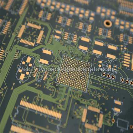
We are a professional High-Speed Materials Substrate manufacturer, we mainly produce ultra-small bump pitch FC BGA substrate, ultra-small trace and spacing packaging substrate and samller gap HDI PCBs.
As of my last knowledge update in January 2022, I don’t have specific information about a term like “High-Speed Materials Substrate” in the context you provided. However, I can offer some general information based on common terminology in electronics and materials science.
In the realm of electronic devices, a substrate refers to the underlying material or surface on which electronic components are mounted or fabricated. High-speed materials substrates are materials deliberately selected or crafted to facilitate the functioning of electronic circuits operating at high frequencies and speeds.
The effectiveness of electronic circuits, particularly in tasks such as high-frequency communication or high-speed data processing, hinges significantly on the characteristics of the underlying substrate material.Key characteristics that high-speed materials substrates often need to possess include:
Low Signal Loss: High-speed applications require materials with low electrical loss to minimize signal degradation as signals pass through the substrate.
Low Dielectric Constant (Dk): The dielectric constant of a material affects the speed at which electrical signals can propagate through it. Lower dielectric constants are often desirable for high-speed applications.
Low Dissipation Factor (Df): This factor measures the efficiency of a material in storing and releasing electrical energy. Low dissipation is crucial for maintaining signal integrity.
High Thermal Conductivity: Electronic devices operating at high speeds generate heat. High thermal conductivity helps in dissipating this heat efficiently, preventing overheating and performance degradation.
Dimensional Stability: The substrate material should maintain its physical and electrical properties under different temperature and humidity conditions to ensure stable performance.
Smooth Surface: A smooth surface is important for the precise placement of electronic components, especially in miniaturized high-frequency circuits.
High-speed substrates commonly leverage specialized materials tailored for the demands of advanced electronic applications. Examples of these materials encompass distinct variations of ceramics, laminates, and composites. Notably, polytetrafluoroethylene (PTFE), ceramic-filled hydrocarbons, and specific varieties of glass-reinforced epoxy laminates are frequently chosen for their performance attributes in high-speed applications.
What is the Role of High-Speed Materials Substrate in PCB Engineering?
In the intricate and dynamic field of PCB engineering, the role of high-speed materials substrate stands out as a critical factor in determining the performance and capabilities of electronic devices. As we embark on this journey through the depths of PCB engineering, we will delve into the profound world of high-speed materials substrate, exploring its definition, functions, types, and the crucial distinctions from traditional PCBs.
Defining High-Speed Materials Substrate
High-speed materials substrate is the unsung hero in the realm of electronic devices. It serves as the foundational layer upon which high-performance circuits are built. Unlike conventional substrates, high-speed materials substrate is specifically designed to meet the demanding requirements of high-frequency and high-speed applications. These substrates are engineered to provide not just a physical base but also to ensure optimal signal integrity and minimal electromagnetic interference.
Functions That Define Excellence
The functions of high-speed materials substrate are multifaceted and crucial for the optimal functioning of electronic components. At the forefront of its functionalities, high-speed materials substrate excels in expediting the transmission of data at unprecedented speeds, a fundamental necessity in the contemporary digital environment. Moreover, this substrate assumes a pivotal responsibility in upholding signal integrity, guaranteeing the resilience and accuracy of signals even when operating at elevated frequencies. The substrate also contributes to minimizing electromagnetic interference, a common challenge in electronic designs.
Exploring the Diverse Types
As we navigate the landscape of high-speed materials substrate, we encounter various types tailored to specific applications. Advanced dielectric materials, engineered laminates, and specialized coatings are just a few examples of the diverse range of materials used in high-speed substrates. Each type is carefully selected based on its unique properties, catering to the specific demands of high-speed electronic designs.
Distinguishing Characteristics from Traditional PCBs
A fundamental aspect of understanding high-speed materials substrate is distinguishing it from traditional PCBs. While traditional PCBs have served as the backbone of electronic devices for decades, the evolution towards high-speed materials substrate represents a paradigm shift in electronic engineering. Comparisons between these substrates shed light on their distinct roles in modern electronics.
The Intricate Structure and Advanced Production Technologies
Peeling back the layers of high-speed materials substrate unveils its intricate structure. This section of the journey also takes us through the advanced production technologies employed in its fabrication. Improved High-Density Interconnect (HDI) fabrication techniques and the evolution of semi-additive methods play a pivotal role in shaping the capabilities of high-speed materials substrate.
Addressing Frequently Asked Questions
To provide a comprehensive understanding, we address frequently asked questions surrounding high-speed materials substrate. From its applications to compatibility considerations, these insights aim to provide clarity for engineers venturing into the realm of high-speed electronics.
Conclusion: A Pivotal Player in PCB Engineering
In conclusion, the significance of high-speed materials substrate in PCB engineering cannot be overstated. As electronic designs continue to push the boundaries of speed and performance, understanding and leveraging advanced materials substrates become paramount for engineers and designers alike. This exploration into the profound world of high-speed materials substrate is a testament to its pivotal role in shaping the future of electronic devices. Every layer, every material, contributes to the intricate tapestry of modern electronics, and high-speed materials substrate stands as a crucial player in this evolving landscape.
What Constitutes High-Speed Materials Substrate?
In the intricate realm of electronic devices, high-speed materials substrate emerges as a concealed hero, silently empowering the seamless operation of high-performance circuits. This article aims to delve deep into the fundamental question: What constitutes high-speed materials substrate? By uncovering its characteristics, applications, and the intricate dance it performs behind the scenes, we seek to demystify this specialized type of substrate designed to meet the demanding requirements of high-frequency and high-speed applications.
Defining High-Speed Materials Substrate
High-speed materials substrate serves as the unsung foundation for the optimal functioning of electronic devices. Unlike conventional substrates, it is intricately designed and tailored to navigate the challenges posed by high-frequency and high-speed applications. These substrates are crafted with precision, considering the unique demands of modern electronics that continually push the boundaries of data transmission speed.
The Silent Hero in Electronic Devices
Often operating behind the scenes, high-speed materials substrate is the silent hero ensuring the cohesiveness and efficiency of high-performance circuits. Its unassuming presence is crucial in enabling the rapid exchange of data, a cornerstone requirement in today’s technology landscape. While electronic devices capture our attention with sleek designs and vibrant displays, it is the high-speed materials substrate that forms the backbone, facilitating the intricate dance of electrons.
Foundation for Seamless Operation
Consider high-speed materials substrate as the bedrock upon which the architecture of high-performance circuits is built. Its specialized nature enables it to act as a conduit for the flow of data, ensuring that information traverses through electronic components with minimal latency. This foundational role is akin to the silent conductor of an orchestra, orchestrating a harmonious symphony of electronic signals.
Tailored for High-Frequency and High-Speed Applications
What sets high-speed materials substrate apart is its adaptability to the demanding requirements of high-frequency and high-speed applications. These substrates are equipped to handle the challenges posed by rapid signal transitions and the intricacies of data transmission in advanced electronic systems. The materials used in their composition are carefully selected to minimize signal loss and interference, ensuring the fidelity of data even at blistering speeds.
Characteristics that Define Excellence
Delving into the specifics, high-speed materials substrate boasts characteristics that define its excellence. The dielectric properties of these substrates are finely tuned to support the propagation of high-frequency signals. Moreover, their impedance control capabilities contribute to maintaining signal integrity, preventing reflections and distortions that can compromise data accuracy.
Applications Across Industries
The versatility of high-speed materials substrate extends its reach across various industries. From telecommunications and aerospace to consumer electronics and medical devices, the demand for high-speed data transmission is ubiquitous. In each of these domains, the substrate plays a critical role in enabling technologies that demand rapid data processing and transmission.
Intricate Design and Manufacturing
Peeling back the layers, we uncover the intricate design and manufacturing processes that contribute to the unique capabilities of high-speed materials substrate. Advanced High-Density Interconnect (HDI) fabrication techniques and the evolution of semi-additive methods are integral in shaping the substrate’s structure. These processes are geared towards achieving finer trace widths and tighter spacings, essential for handling high-frequency signals.
The Intersection with Traditional PCBs
Understanding high-speed materials substrate necessitates a comparison with traditional PCBs. While traditional PCBs have been stalwarts in electronic engineering, the evolution towards high-speed materials substrate reflects the growing need for enhanced data transmission capabilities. Contrasting the two provides insights into their respective roles and underscores the paradigm shift occurring in electronic design.
The Future Landscape
As we navigate through the intricate world of high-speed materials substrate, it is evident that this specialized substrate is not just a technological necessity but a harbinger of the future. As electronic devices continue to evolve, demanding faster and more efficient data processing, high-speed materials substrate will remain at the forefront of innovation, ensuring the seamless integration of advanced technologies.
Conclusion: Unmasking the Unsung Hero
In conclusion, high-speed materials substrate emerges from the shadows as the unsung hero in the narrative of electronic devices. Its role in facilitating high-speed data transmission, maintaining signal integrity, and serving as the foundation for cutting-edge electronic circuits cannot be overstated. This exploration into the constitution of high-speed materials substrate unveils its significance, making it clear that its silent contributions resonate across the spectrum of electronic engineering. As we peer into the future, it is certain that high-speed materials substrate will continue to be a driving force, propelling the evolution of electronic devices into realms yet unexplored.
What Functions Does High-Speed Materials Substrate Serve?
In the ever-evolving landscape of electronic engineering, high-speed materials substrate takes center stage, offering a multifaceted array of functions that extend beyond merely providing a physical base for electronic components. This article delves into the intricate world of high-speed materials substrate, unraveling its diverse functions, which include playing a pivotal role in signal integrity, minimizing electromagnetic interference, and supporting the ultra-fast transmission of data. Through this exploration, we aim to shed light on the nuanced functionalities that make high-speed materials substrate an indispensable component in the design and performance of advanced electronic devices.
Foundational Support for Electronic Components
At its core, high-speed materials substrate serves as the foundational support for electronic components within a device. It provides a stable and robust platform upon which intricate circuits, semiconductor devices, and other electronic elements can be securely mounted. This foundational role is analogous to the framework of a building, ensuring the structural integrity and coherence of the entire electronic system.
Signal Integrity: Ensuring Robust and Accurate Signals
One of the primary functions that set high-speed materials substrate apart is its critical role in maintaining signal integrity. Signal integrity refers to the quality of signals as they traverse through the substrate and electronic components. In high-speed applications, where data is transmitted at rapid rates, preserving signal integrity becomes paramount.
High-speed materials substrate achieves this by carefully controlling the impedance of the transmission lines. Impedance matching is crucial to prevent signal reflections, distortions, and other phenomena that can degrade the quality of signals.The substrate’s capacity to uphold a steady and regulated impedance significantly contributes to the dependability of data transmission. This, consequently, ensures the precise and optimal functioning of electronic devices.
Minimizing Electromagnetic Interference (EMI)
The occurrence of electromagnetic interference (EMI) is a common challenge encountered in electronic systems, particularly in situations characterized by high-frequency applications.EMI occurs when the electromagnetic fields generated by a particular electronic component interfere with the regular operation of nearby components.High-speed materials substrate acts as a shield, mitigating EMI by providing effective electromagnetic isolation between different sections of the electronic circuit.
The substrate’s design includes features that minimize the coupling of electromagnetic fields between adjacent traces and components. By reducing EMI, high-speed materials substrate enhances the overall electromagnetic compatibility of electronic devices, preventing unwanted interference that could compromise their performance.
Supporting Ultra-Fast Data Transmission
Perhaps one of the most critical functions of high-speed materials substrate is its ability to support the ultra-fast transmission of data. In today’s digital landscape, where the demand for high-speed communication is relentless, the substrate plays a pivotal role in facilitating the rapid exchange of information.
The composition of high-speed materials substrate is tailored to accommodate high-frequency signals. Advanced dielectric materials with low loss characteristics are employed to minimize attenuation and ensure that signals can travel across the substrate with minimal degradation. Additionally, the substrate’s design incorporates features such as controlled impedance, optimized trace layouts, and advanced manufacturing techniques like High-Density Interconnect (HDI), all contributing to the substrate’s capability to support ultra-fast data transmission.
Advanced Manufacturing Techniques: The Key to Functionality
The multifaceted functions of high-speed materials substrate are intricately tied to advanced manufacturing techniques. Improved HDI fabrication technologies and the evolution of semi-additive methods have played a pivotal role in enhancing the functionality of high-speed materials substrate.
Improved HDI fabrication involves densely packing components and traces in a smaller footprint, reducing parasitic capacitance and inductance. This not only enhances the overall performance of the substrate but also supports the efficient transmission of high-frequency signals. The semi-additive method, on the other hand, allows for finer trace patterns and tighter spacings, contributing to the substrate’s capability to minimize signal loss and interference.
Applications Across Industries: A Testament to Versatility
The multifunctionality of high-speed materials substrate extends its reach across diverse industries. In telecommunications, it enables the rapid exchange of data in high-speed networks. In aerospace, it supports avionics systems that demand reliability and precision. In consumer electronics, it facilitates the seamless operation of devices that rely on high-speed data processing. The versatility of high-speed materials substrate is a testament to its ability to meet the unique demands of various applications.
Addressing Frequently Asked Questions: Enhancing Understanding
In the quest to enhance understanding, addressing frequently asked questions (FAQs) surrounding high-speed materials substrate becomes imperative. From inquiries about its applications to considerations for engineers, this section aims to provide clarity and insights that contribute to a more comprehensive understanding of the substrate’s functions.
Conclusion: The Heartbeat of High-Performance Electronics
In conclusion, the functions performed by high-speed materials substrate are the heartbeat of high-performance electronics. Its multifaceted role in providing foundational support, ensuring signal integrity, minimizing electromagnetic interference, and supporting ultra-fast data transmission collectively defines its indispensability in electronic engineering. As we navigate the intricate world of advanced technologies, high-speed materials substrate stands as a silent yet powerful enabler, driving the evolution of electronic devices into realms of speed and efficiency previously unattainable. The ongoing innovation in manufacturing techniques and the continual refinement of substrate designs underscore its central role in shaping the future of electronic engineering.
What Are the Different Types of High-Speed Materials Substrate?
In the dynamic landscape of high-speed electronics, the substrates that underpin these advanced systems are as diverse as the applications they serve. This article embarks on a journey to unravel the intricate world of high-speed materials substrate, exploring the myriad types tailored to meet the specific demands of high-speed electronic designs. From advanced dielectric materials to meticulously engineered laminates, each type contributes uniquely to the evolving fabric of electronic engineering.
Advanced Dielectric Materials: The Foundation of High-Speed Signal Transmission
At the core of high-speed materials substrate lies the category of advanced dielectric materials. These materials serve as the foundation for efficient signal transmission in high-frequency applications. Engineered to have low dielectric constant and low loss tangent, advanced dielectrics minimize signal attenuation and distortion, enabling signals to propagate across the substrate with minimal interference. Materials such as polytetrafluoroethylene (PTFE), liquid crystal polymer (LCP), and various high-performance ceramics exemplify this class of substrates, each chosen for its specific electrical properties and application requirements.
Engineered Laminates: Tailoring Substrates for Specific Applications
Within the realm of high-speed materials substrate, engineered laminates emerge as versatile players, providing a tailored approach to substrate design. These laminates consist of layers of different materials, each chosen for its unique characteristics. For instance, a typical engineered laminate might comprise a core layer with high dielectric constant for signal integrity and outer layers with lower dielectric constants for controlled impedance. The meticulous layering enables the substrate to meet specific impedance and electrical performance requirements, making engineered laminates a preferred choice in applications demanding precise control over signal propagation.
Flexible Substrates: Navigating the Demands of Modern Electronics
As electronic devices continue to shrink in size and evolve in form factor, flexible substrates have become increasingly vital.Constructed primarily from flexible polymer materials, these substrates enable the development of electronic components that can be bent and folded. The utilization of flexible substrates presents notable advantages in various applications, including wearable technology, medical devices, and flexible displays, where the application of conventional rigid substrates may be deemed impractical. Key materials commonly employed in the fabrication of flexible substrates encompass polyimide and polyester, delivering a combination of flexibility, thermal stability, and electrical performance.
Metal Core Substrates: Enhancing Thermal Performance
In applications where efficient heat dissipation is paramount, metal core substrates come into play.These substrates incorporate a metal layer, usually made of aluminum or copper, positioned between layers of dielectric material. Functioning as a heat sink, the metal layer effectively dissipates the heat produced by electronic components.Metal core substrates find applications in power electronics, high-brightness LED lighting, and other scenarios where thermal management is critical. The choice of metal and dielectric materials can be tailored to achieve specific thermal conductivity and electrical performance requirements.
Glass-Reinforced Substrates: Balancing Rigidity and Electrical Performance
In situations where rigidity and dimensional stability are essential, glass-reinforced substrates offer a compelling solution. These substrates incorporate glass fibers into the base material, enhancing mechanical strength and stability. Glass-reinforced substrates strike a balance between structural integrity and electrical performance, making them suitable for applications such as automotive electronics, industrial controls, and harsh environments where the substrate may be subjected to mechanical stress.
Ceramic Substrates: Merging High Thermal Conductivity with Electrical Insulation
Ceramic substrates emerge as a distinctive category, combining high thermal conductivity with electrical insulation. Alumina (aluminum oxide) and aluminum nitride are common ceramic materials used in these substrates. Ceramic substrates find favor in power electronics and high-frequency applications where efficient heat dissipation is crucial, and electrical insulation is paramount. The inherent properties of ceramics contribute to their reliability in demanding environments, making them suitable for applications ranging from automotive power modules to telecommunications infrastructure.
Integrated Passive Devices (IPDs): Consolidating Functionality in the Substrate
A notable trend in high-speed materials substrate is the integration of passive components directly into the substrate, giving rise to Integrated Passive Devices (IPDs). IPDs consolidate functions such as resistors, capacitors, and inductors within the substrate itself, offering advantages in terms of size reduction, reduced parasitic effects, and enhanced overall system performance. The integration of passive components into the substrate aligns with the ongoing trend towards miniaturization and increased functionality in electronic devices.
Organic Substrates: Embracing Environmental Considerations
In the pursuit of environmentally conscious electronic design, organic substrates based on materials like organic laminates and bio-based resins have gained traction. These substrates offer a more sustainable alternative to traditional materials, reducing the environmental impact of electronic devices. Organic substrates find applications in various consumer electronics, contributing to the broader industry push toward eco-friendly and recyclable materials.
Tailoring Substrates to Application Needs
The diversity of high-speed materials substrate types underscores the importance of tailoring substrate selection to the specific needs of the application. The choice of substrate influences factors such as signal integrity, thermal management, flexibility, and environmental impact. Engineers must carefully consider these factors to optimize the performance and reliability of electronic systems in diverse applications.
Advanced Manufacturing Techniques: Crafting the Future of Substrates
The production of high-speed materials substrates is intricately tied to advanced manufacturing techniques. Techniques such as laser drilling, chemical etching, and additive manufacturing contribute to the precision and complexity required for high-speed applications. As manufacturing technologies continue to evolve, substrates can be crafted with increasingly finer features, allowing for enhanced performance in demanding electronic designs.
Conclusion: Navigating the Complex Landscape of High-Speed Materials Substrate
In conclusion, the diverse landscape of high-speed materials substrate reflects the ever-evolving demands of electronic engineering. From advanced dielectric materials that ensure signal integrity to flexible substrates accommodating modern form factors, each substrate type brings a unique set of characteristics to the table. The intricacies of substrate selection play a pivotal role in determining the success of electronic designs, influencing factors ranging from electrical performance to environmental sustainability. As we navigate this complex landscape, it becomes clear that the future of high-speed electronics is intricately woven into the diverse tapestry of high-speed materials substrate types, each contributing to the advancement of electronic technology in its own distinctive way.
How Does High-Speed Materials Substrate Differ from Traditional PCBs?
In the ever-evolving landscape of electronic engineering, the distinction between high-speed materials substrate and traditional printed circuit boards (PCBs) stands as a testament to the dynamic progression of technology. This exploration seeks to shed light on the nuances that set high-speed materials substrate apart from its conventional counterparts, such as printed wiring boards (PWBs) and standard PCBs. By drawing comparisons and highlighting their diverse roles, we embark on a journey through the intricate tapestry of modern electronics.
Evolution in Design and Functionality
The fundamental divergence between high-speed materials substrate and traditional PCBs lies in the evolution of design and functionality. High-speed materials substrate is purposefully engineered to meet the demands of cutting-edge electronic designs, especially those involving high-frequency applications. This specialized substrate undergoes meticulous design considerations to minimize signal loss, maintain signal integrity, and address challenges associated with rapid signal transitions.
In contrast, traditional PCBs, including printed wiring boards (PWBs), have historically served as the bedrock of electronic devices, handling a wide range of applications. While conventional PCBs excel in many scenarios, the evolution towards high-speed materials substrate signifies a shift towards more intricate and demanding electronic designs.
Material Composition and Dielectric Properties
A key distinguishing factor is the material composition and dielectric properties of high-speed materials substrate compared to traditional PCBs. High-speed materials substrate employs advanced dielectric materials, such as polytetrafluoroethylene (PTFE) and liquid crystal polymer (LCP), which exhibit low dielectric constant and low loss tangent. These characteristics are tailored to support high-frequency signals, minimizing signal distortion and ensuring efficient data transmission.
Conventional PCBs, on the other hand, may utilize standard materials like FR-4 (Flame Retardant 4) with comparatively higher dielectric constants. While suitable for many applications, these materials may introduce more significant signal losses at higher frequencies, making them less optimal for high-speed electronic designs.
Impedance Control and Signal Integrity
Impedance control and signal integrity are critical considerations in high-frequency applications, and here lies another differentiating factor. High-speed materials substrate is meticulously designed to provide precise impedance control, minimizing reflections and maintaining signal integrity. This is achieved through careful selection of materials, controlled trace widths, and optimized layer stacking.
Traditional PCBs, while offering satisfactory impedance control in moderate-frequency applications, may exhibit challenges in maintaining stringent control at higher frequencies. The evolving demands of modern electronics, especially in areas like telecommunications and high-speed data transmission, necessitate the heightened impedance control offered by specialized high-speed materials substrate.
Manufacturing Techniques: Precision in Every Layer
The manufacturing techniques employed in crafting high-speed materials substrate underscore the precision required in its production. Improved High-Density Interconnect (HDI) fabrication techniques and advanced semi-additive methods allow for finer trace patterns, reduced parasitics, and increased layer density. These techniques enable the intricate designs necessary to support high-frequency signals and precise impedance matching.
While traditional PCBs also benefit from advancements in manufacturing, the level of precision required for high-speed applications often exceeds the capabilities of standard fabrication processes. High-speed materials substrate, with its emphasis on finer features and reduced parasitics, showcases the advancements pushing the boundaries of electronic manufacturing.
Applications and Industry Trends
Examining the applications and industry trends provides a broader perspective on the divergence between high-speed materials substrate and traditional PCBs. High-speed materials substrate is specifically tailored for applications requiring swift data processing, exemplified in crucial domains like telecommunications infrastructure, high-performance computing, and advanced driver-assistance systems within automotive electronics.
While traditional PCBs remain integral to a diverse range of applications, spanning from consumer electronics to industrial controls, the rising demand for high-speed data transmission and processing underscores the growing importance of specialized high-speed materials substrate. As industries increasingly seek innovation and efficiency, the unique capabilities offered by high-speed materials substrate become paramount, driving advancements and setting the stage for transformative developments across various sectors.
Flexibility and Form Factor: Adapting to Modern Needs
The flexibility and form factor of high-speed materials substrate represent a paradigm shift from the rigidity of traditional PCBs. High-speed materials substrate, often designed with flexible polymer materials like polyimide, opens the door to bendable and foldable electronic components. This adaptability is particularly valuable in applications such as wearable technology, medical devices, and flexible displays, where the traditional rigid form of PCBs may limit design possibilities.
Traditional PCBs, while offering structural integrity, may struggle to meet the demands of applications requiring intricate form factors. The flexibility of high-speed materials substrate aligns with the evolving trend towards miniaturization and the integration of electronics into unconventional shapes and surfaces.
Reliability and Environmental Considerations
Reliability and environmental considerations represent an integral aspect of the comparison between high-speed materials substrate and traditional PCBs. High-speed materials substrate, designed with a focus on signal integrity and reduced signal loss, enhances the overall reliability of electronic systems, especially in high-frequency and high-speed applications.
Traditional PCBs, renowned for their reliability in various applications, may face challenges in environments where the demands on signal integrity are more stringent. Additionally, the choice of materials in high-speed materials substrate, including eco-friendly options like bio-based resins, aligns with the growing emphasis on sustainability in electronic design.
Conclusion: Forging the Future of Electronics
In conclusion, distinguishing high-speed materials substrate from traditional PCBs provides insight into the ongoing evolution of electronic engineering. The specialized design, material composition, manufacturing techniques, and adaptability of high-speed materials substrate cater to the demands of modern electronics, where high-frequency applications and intricate form factors are increasingly prevalent.
While traditional PCBs continue to serve admirably in many applications, the emergence of high-speed materials substrate signals a shift towards precision, adaptability, and enhanced performance. The nuanced roles played by these substrates in the intricate tapestry of modern electronics underscore their significance in forging the future of electronic design and technology. As we navigate this dynamic landscape, the synergy between high-speed materials substrate and traditional PCBs will continue to shape the trajectory of electronic engineering, propelling innovation to new heights.
What Constitutes the Main Structure and Production Technologies of High-Speed Materials Substrate?
Embarking on a journey into the heart of electronic innovation, we peel back the layers to unravel the intricate structure of high-speed materials substrate. This exploration not only unveils the essential components that constitute the substrate’s main structure but also delves into the cutting-edge production technologies that drive its evolution. From Improved High-Density Interconnect (HDI) fabrication techniques to the transformative advancements in semi-additive methods, this comprehensive dive seeks to shed light on the intricacies that make high-speed materials substrate a cornerstone in modern electronic engineering.
The Core Structure of High-Speed Materials Substrate
At its essence, the main structure of high-speed materials substrate is a carefully orchestrated combination of layers, each playing a distinct role in ensuring optimal performance in high-frequency applications. These layers can be categorized into:
- Foundational Layer: Acting as the cornerstone, this pivotal stratum comprises premium dielectric materials meticulously selected for their minimal dielectric constant and low loss tangent. Standard materials found in this foundational layer encompass polytetrafluoroethylene (PTFE), liquid crystal polymer (LCP), and advanced ceramics, with the selection tailored to the precise demands of the application in question.
- Conductive Layers: Sandwiched between dielectric layers are conductive traces, meticulously designed to transmit signals with minimal loss. Copper is a prevalent choice for these conductive layers due to its excellent conductivity and compatibility with standard manufacturing processes.
- Ground and Power Planes: Strategically positioned ground and power planes contribute to the substrate’s overall performance by providing a stable reference for signals and facilitating efficient power distribution. These planes play a crucial role in minimizing electromagnetic interference and maintaining signal integrity.
- Protective Solder Mask: Covering the conductive layers, the solder mask serves a protective role, guarding against environmental factors and preventing unintended electrical contact. This layer is especially critical in ensuring the reliability and longevity of the substrate.
- Surface Finish: The topmost layer, the surface finish, influences solderability and overall reliability. Common surface finishes include gold, tin, or nickel, each chosen based on factors such as cost, compatibility, and specific application requirements.
Improved High-Density Interconnect (HDI) Fabrication Techniques
The evolution of Improved High-Density Interconnect (HDI) fabrication techniques marks a significant stride in enhancing the capabilities of high-speed materials substrate. This methodology focuses on achieving higher circuit density and finer features, allowing for more intricate and compact designs. Key elements of Improved HDI fabrication include:
- Fine Line and Spacing: Improved HDI techniques enable the creation of finer lines and spacing between conductive traces. This increased precision is vital in accommodating the demands of high-frequency signals, minimizing parasitic capacitance and inductance.
- Microvias: HDI facilitates the integration of microvias, tiny holes that connect different layers of the substrate. Microvias contribute to the reduction of signal propagation delays and enhance the overall electrical performance of the substrate.
- Sequential Build-Up (SBU): SBU is a technique where layers are added sequentially, allowing for the creation of complex multilayer structures. This approach offers flexibility in design and supports the integration of various materials with distinct electrical properties.
- Via-in-Pad Technology: In high-speed applications, the placement of vias directly within component pads becomes crucial for optimizing signal paths. Improved HDI techniques enable the implementation of Via-in-Pad technology, enhancing signal integrity and facilitating more compact designs.
Evolution of Semi-Additive Methods
The evolution of semi-additive methods represents a revolutionary leap in substrate fabrication, further elevating the capabilities of high-speed materials substrate. Semi-additive methods involve selectively adding material to the substrate, enabling greater precision and complexity. Key aspects of this evolution include:
- Selective Plating: Semi-additive methods allow for selective plating, where conductive material is deposited only in specific areas. This precision is instrumental in achieving intricate circuit patterns and addressing the challenges associated with high-frequency signals.
- Laser Ablation: Laser ablation is employed to selectively remove material from the substrate, defining the circuit pattern with unparalleled accuracy. This technique contributes to the creation of finer features, reducing parasitic effects and supporting the demands of high-speed applications.
- Thin Film Deposition: Semi-additive methods facilitate the deposition of thin films with precise thickness, enhancing the performance of conductive and dielectric layers. This level of control is crucial for achieving the desired electrical properties in high-speed materials substrate.
- Embedded Components: The evolution of semi-additive methods opens the door to embedding passive components directly within the substrate. This integration minimizes signal paths, reduces parasitics, and contributes to the overall miniaturization of electronic devices.
Future Trends: Beyond Current Innovations
As we delve into the main structure and production technologies of high-speed materials substrate, it becomes evident that ongoing innovations continue to shape the landscape of electronic engineering. Future trends in substrate fabrication are poised to explore:
- Advanced Materials: Continued research into materials with enhanced electrical properties, thermal stability, and environmental sustainability will drive the development of high-speed materials substrate.
- 3D Integration: The exploration of three-dimensional integration techniques holds promise for further optimizing space utilization, reducing signal propagation distances, and supporting more complex electronic designs.
- Advanced Packaging: Innovations in packaging technologies, including System-in-Package (SiP) and heterogeneous integration, will likely play a pivotal role in enhancing the performance of high-speed materials substrate in integrated circuits.
- Quantum Advances: As the field of quantum computing progresses, high-speed materials substrate may find applications in the development of quantum processors, pushing the boundaries of computing capabilities.
Conclusion: Paving the Way for Advanced Electronics
In conclusion, peeling back the layers of high-speed materials substrate reveals a realm of precision, innovation, and adaptability. The intricate main structure, coupled with the evolution of production technologies like Improved HDI and semi-additive methods, positions high-speed materials substrate at the forefront of electronic engineering.
As demands for high-speed data transmission and processing intensify, the ongoing advancements in substrate fabrication underscore its crucial role in driving innovation across various industries. Looking ahead, the trajectory of electronic design holds the promise of revolutionary advancements that will redefine the boundaries of performance and functionality. In this dynamic landscape, future trends are poised to usher in a new era of electronic engineering, pushing the envelope of innovation. At the forefront of this evolution stands high-speed materials substrate, a symbol of unwavering commitment to excellence in the ever-evolving pursuit of advancing electronic technologies.
What Are the Frequently Asked Questions About High-Speed Materials Substrate?
As the demand for high-speed data transmission and processing continues to rise, so does the curiosity surrounding high-speed materials substrate—an essential component in the intricate tapestry of modern electronics. This section seeks to address common questions, providing insights into the applications, compatibility, and considerations for engineers entering the realm of high-speed electronics. Let’s embark on a journey to unravel the frequently asked questions surrounding high-speed materials substrate and shed light on its pivotal role in shaping the future of electronic engineering.
What are the Key Applications of High-Speed Materials Substrate?
High-speed materials substrate finds applications in a spectrum of industries where rapid data transmission and processing are paramount. Key applications include:
- Telecommunications: Facilitating swift data transmission within the realm of telecommunications infrastructure, inclusive of cutting-edge networks such as 5G and beyond.
- Consumer Electronics: Empowering the development of devices with enhanced data processing capabilities, spanning a range of gadgets such as smartphones, tablets, and smartwatches.
- Automotive Electronics: Enabling sophisticated driver-assistance systems (ADAS) and fostering communication networks within vehicles.
- Aerospace and Defense: Powering avionics systems and defense electronics that demand reliability and high performance.
- Industrial Controls: Contributing to the efficiency of industrial automation systems and control electronics.
- Medical Devices: Enhancing the functionality of medical equipment that relies on rapid data processing.
How Does High-Speed Materials Substrate Differ from Traditional PCBs?
High-speed materials substrate differs from traditional printed circuit boards (PCBs) in several key aspects:
- Material Composition: High-speed materials substrate often incorporates advanced dielectric materials with low dielectric constants, tailored for high-frequency applications.
- Impedance Control: Precision impedance control is a critical feature of high-speed materials substrate, ensuring signal integrity in high-frequency designs.
- Manufacturing Techniques: Specialized manufacturing techniques, such as Improved High-Density Interconnect (HDI) and semi-additive methods, set high-speed materials substrate apart in terms of precision and complexity.
Is High-Speed Materials Substrate Compatible with Standard Manufacturing Processes?
Yes, high-speed materials substrate is compatible with standard manufacturing processes, albeit with certain modifications and advancements. The incorporation of technologies like Improved HDI and semi-additive methods has allowed for the integration of high-speed materials substrate into standard manufacturing workflows. These adaptations ensure that the benefits of high-speed materials substrate can be realized without necessitating a complete overhaul of existing manufacturing practices.
What Considerations Should Engineers Keep in Mind when Designing with High-Speed Materials Substrate?
Engineers venturing into high-speed electronics should consider the following key factors:
- Signal Integrity: Ensuring the design minimizes signal loss and distortion to maintain signal integrity, especially in high-frequency applications.
- Impedance Matching: Precision impedance matching is crucial for preventing signal reflections and optimizing data transmission.
- Thermal Management: Adequate thermal considerations, especially in applications with high power density, to prevent overheating and ensure reliability.
- Advanced Manufacturing Techniques: Leveraging advanced techniques like Improved HDI and semi-additive methods for intricate designs and optimal performance.
Can High-Speed Materials Substrate Support Flexible and Bendable Designs?
Yes, high-speed materials substrate can support flexible and bendable designs.The utilization of flexible polymer materials, exemplified by polyimide and polyester, enables the development of electronic components with the unique capability to bend and fold. This inherent flexibility proves especially advantageous in applications such as wearable technology and flexible displays, where the constraints of traditional rigid substrates may pose impractical limitations.
How Does High-Speed Materials Substrate Contribute to Signal Integrity?
High-speed materials substrate contributes to signal integrity through several mechanisms:
- Controlled Impedance: Precise control of impedance along signal paths minimizes signal reflections, ensuring consistent and reliable data transmission.
- Reduced Crosstalk: Careful layout and design considerations help minimize electromagnetic crosstalk between adjacent traces, preserving signal quality.
- Low Loss Tangent: The use of materials with low loss tangent minimizes signal attenuation, allowing signals to propagate with minimal distortion.
Are There Environmental Considerations in the Use of High-Speed Materials Substrate?
Yes, environmental considerations are increasingly important in electronic design. High-speed materials substrate can incorporate eco-friendly options, such as bio-based resins, contributing to more sustainable electronic products. The industry is moving towards adopting materials and manufacturing processes that minimize environmental impact, aligning with the broader push for greener and more responsible technology.
How Does High-Speed Materials Substrate Contribute to Miniaturization in Electronics?
High-speed materials substrate contributes to miniaturization by enabling:
- Fine Feature Integration: Improved HDI and semi-additive methods allow for finer trace patterns and reduced parasitics, facilitating the integration of more components in a smaller footprint.
- Embedded Components: The evolution of semi-additive methods enables the embedding of passive components directly within the substrate, reducing the overall size of the electronic system.
Conclusion: Navigating the Complexities of High-Speed Materials Substrate
In navigating the complexities of high-speed materials substrate, addressing frequently asked questions provides a foundation for understanding its applications, capabilities, and considerations. As the relentless march of technology continues, high-speed materials substrate stands as a linchpin in the world of high-speed electronics, facilitating advancements across diverse industries. Engineers, armed with insights into the intricacies of high-speed materials substrate, can navigate the challenges and unlock the full potential of this critical component in shaping the future of electronic engineering.
Why is High-Speed Materials Substrate Crucial in PCB Engineering?
In the dynamic world of PCB engineering, the pivotal role of high-speed materials substrate cannot be emphasized enough. As electronic designs soar to new heights in speed and performance, the comprehension and utilization of advanced materials substrates become indispensable for engineers and designers alike. This exploration into the realm of high-speed materials substrate offers more than just a glimpse; it unveils the essence of its significance in shaping the future of electronic devices.
Enabling Unprecedented Data Processing Speeds
At the heart of the matter lies the unparalleled capability of high-speed materials substrate to facilitate unprecedented data processing speeds. At the core of its functionality, high-speed materials substrate relies on sophisticated dielectric materials like polytetrafluoroethylene (PTFE) and liquid crystal polymer (LCP), playing a pivotal role in mitigating signal loss and distortion. This characteristic holds paramount significance as it addresses the ever-increasing requirements for swift and effective data transmission, especially in realms such as 5G telecommunications, high-performance computing, and advanced driver-assistance systems (ADAS).
Precision Impedance Control for Signal Integrity
One of the defining features that elevate high-speed materials substrate to a position of prominence is its ability to offer precision impedance control. In the intricate world of high-frequency applications, maintaining signal integrity is paramount. The substrate’s meticulous design ensures that impedance is precisely controlled along signal paths, minimizing reflections and optimizing data transmission. This level of control is fundamental in mitigating signal distortions that can impede the performance of electronic systems.
Tailored Material Composition for High-Frequency Challenges
The material composition of high-speed materials substrate stands as a testament to its adaptability to the challenges posed by high-frequency applications. Unlike traditional PCBs that may utilize standard materials like FR-4, high-speed materials substrate incorporates advanced dielectrics with low dielectric constants and low loss tangents. This tailored material selection is a strategic response to the increasing prevalence of high-frequency signals, ensuring optimal performance and reliability.
Advanced Manufacturing Techniques for Precision
The significance of high-speed materials substrate is further underscored by the advanced manufacturing techniques employed in its production. Improved High-Density Interconnect (HDI) fabrication techniques and the evolution of semi-additive methods enable the creation of finer trace patterns, reduced parasitics, and increased layer density. These techniques contribute to the substrate’s precision, allowing for intricate designs that align with the exacting requirements of high-speed applications.
The Role in Future Innovations
Looking forward, high-speed materials substrate is poised to play a pivotal role in future innovations within the realm of PCB engineering. As electronic designs continue to evolve, trends such as 3D integration, advanced packaging technologies, and the exploration of new materials will shape the landscape. High-speed materials substrate, with its inherent adaptability and precision, stands ready to contribute to these innovations, pushing the boundaries of what is achievable in electronic engineering.
Shaping the Future of Electronic Devices
In conclusion, the significance of high-speed materials substrate in PCB engineering transcends its immediate applications. It serves as a linchpin in the relentless pursuit of pushing the boundaries of electronic devices. As electronic designs become increasingly sophisticated, the role of high-speed materials substrate becomes not just important but indispensable. Engineers and designers must embrace the potential of advanced substrates to unlock new possibilities and usher in a future where speed, performance, and reliability are at the forefront of electronic innovation.
Navigating the Evolving Landscape
This exploration into the realm of high-speed materials substrate is not merely a glimpse but an acknowledgment of its pivotal role in navigating the evolving landscape of PCB engineering. It is a call to engineers and designers to delve deeper into the intricacies of substrate design, to understand how each layer contributes to the overall performance of electronic devices. In this dynamic journey, high-speed materials substrate emerges as a beacon, guiding the way towards a future where electronic devices not only meet but exceed the expectations of speed and efficiency. As we move forward, the collaboration between engineers and advanced substrates will continue to shape the trajectory of PCB engineering, setting the stage for electronic devices that push the boundaries of what was once deemed possible.