
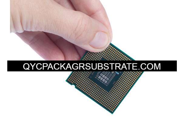
High speed mixed dielectric PCB
High-Speed Mixed Dielectric PCBs Manufacturing, We have the Mitsubishi BT materials, Panasonic Megatron materials, ABF materials, and other types High speed mixed dielectric materials, we offer High speed PCBs from 2 layer to 50 layers. High-Speed Mixed Dielectric PCBs are advanced printed circuit boards engineered to manage high-frequency signals effectively. These PCBs incorporate a combination of different dielectric materials within their substrate layers, strategically selected to optimize signal transmission, impedance matching, and signal integrity. By utilizing various dielectric constants, High-Speed Mixed Dielectric PCBs minimize signal distortion, crosstalk, and electromagnetic interference, crucial for high-speed electronic devices like data servers, networking equipment, and telecommunications systems. Their precise design, including controlled impedance routing and proper grounding techniques, ensures reliable performance in demanding applications. Manufacturing High-Speed Mixed Dielectric PCBs involves specialized processes, including layer stackup design, material selection, and advanced fabrication techniques. With their ability to maintain signal integrity at high frequencies, High-Speed Mixed Dielectric PCBs play a vital role in enabling the efficient operation of modern electronic systems.
What is a High-Speed Mixed Dielectric PCB?
We are a professional High speed mixed dielectric PCB manufacturing supplier, we mainly produce ultra-small bump pitch substrate, ultra-small trace and spacing packaging substrate and PCBs.
A High-Speed Mixed Dielectric PCB (Printed Circuit Board) is a type of PCB designed to accommodate both high-speed and mixed signal components. Here’s a breakdown of its key components and characteristics:
- High-Speed Signals: These are signals that operate at high frequencies, typically in the range of several megahertz (MHz) to several gigahertz (GHz). Examples include signals for data transmission, clock signals, and high-frequency analog signals. High-speed signals require special care in PCB design to prevent signal degradation, such as controlled impedance routing and minimizing signal reflections.
- Mixed Signal: Mixed signal refers to a combination of analog and digital signals on the same PCB. This could include digital data lines alongside analog sensor inputs or output lines. Mixed signal PCBs require careful consideration of signal integrity and noise management to prevent interference between analog and digital signals.
- Dielectric Materials: Dielectric materials are insulating materials used between conductive layers in a PCB to provide electrical isolation and mechanical support. In a mixed dielectric PCB, different dielectric materials may be used for different purposes. For example, high-speed signal traces might require materials with specific dielectric properties to maintain signal integrity, while other sections of the PCB may use different dielectric materials optimized for other characteristics such as cost or mechanical strength.
- Design Considerations: Designing a high-speed mixed dielectric PCB involves considerations such as impedance matching, signal routing, ground plane design, and minimizing signal crosstalk. Specialized CAD tools and simulation software are often used to optimize the design and ensure signal integrity.
- Applications: High-speed mixed dielectric PCBs are commonly used in applications where both high-speed digital and analog signals coexist, such as telecommunications equipment, networking hardware, high-performance computing systems, and instrumentation.
Overall, high-speed mixed dielectric PCBs are essential for maintaining signal integrity and performance in complex electronic systems that require both high-speed digital and analog signal processing.
High speed mixed dielectric PCB manufacturing
What are the PCB Design Guidelines for High-Speed Mixed Dielectric PCBs?
The design guidelines for high-speed mixed dielectric PCBs include the following aspects:
- Controlled Impedance: Ensuring impedance matching of signal traces is crucial. Use appropriate widths and spacing to control the impedance of signal traces, preventing signal reflections and attenuation.
- Signal Routing: Route high-speed signal traces as directly as possible, minimizing bends and branches. Avoid crossing high-speed signal traces with lines carrying high power or noise.
- Ground Plane Design: Ensure a good ground plane to provide an effective return path for signals and minimize signal loops. Maintain good ground isolation between high-speed and analog signal sections.
- Signal Layer Stackup: Select appropriate signal layer stackup based on design requirements. Use lower-loss dielectrics for high-speed signals and minimize differences in dielectric thickness between signal layers.
- Power and Ground Pins: Place power and ground pins close to the devices they power or ground to minimize impedance in the power and ground return paths.
- Crosstalk Mitigation: Take measures to reduce crosstalk between signal traces, such as proper signal spacing, differential pair routing, and the use of shielding layers.
- Simulation and Validation: Validate the design using simulation tools and make necessary adjustments to ensure it meets performance requirements.
- Thermal Management: Consider thermal requirements in PCB design, especially for high-power devices and high-density layouts.
- Package Selection: Choose appropriate packages and components to meet electrical and mechanical requirements of the design, considering thermal characteristics and layout density.
- Avoiding Electromagnetic Compatibility (EMC) Issues: Follow best practices for electromagnetic compatibility, such as proper handling of high-speed signals, minimizing distance between radiating and sensitive areas, and using filters and shielding.
These guidelines help ensure that the design of high-speed mixed dielectric PCBs maintains good signal integrity and performance while minimizing signal interference and other electrical issues.
What is the High-Speed Mixed Dielectric PCB Fabrication Process?
The fabrication process for high-speed mixed dielectric PCBs involves several key steps:
- Design Preparation: Prepare the PCB design layout using specialized PCB design software. Ensure that the design adheres to the high-speed mixed dielectric requirements, including controlled impedance routing, signal layer stackup, and ground plane design.
- Material Selection: Choose appropriate PCB materials for the specific requirements of the high-speed mixed dielectric design. This includes selecting dielectric materials with suitable properties for maintaining signal integrity and minimizing losses at high frequencies.
- Panelization: Arrange multiple PCB designs onto larger panels for efficient manufacturing. Panelization helps optimize material usage and reduces fabrication costs.
- Layer Stackup Preparation: Determine the layer stackup configuration based on the design requirements. This involves specifying the number of signal layers, ground planes, and power planes, as well as the order and thickness of each layer.
- Prepreg and Core Material Lamination: Prepreg (pre-impregnated) and core materials are laminated together to form the multilayer PCB stackup. This process involves applying heat and pressure to bond the layers into a single structure.
- Drilling: Precision drilling is performed to create holes for vias and component mounting pads. Advanced drilling techniques may be used to ensure accurate hole placement and size.
- Through-Hole Plating: Through-hole plating is applied to the drilled holes to create electrical connections between layers. This process involves depositing conductive material, typically copper, onto the hole walls through electroplating.
- Circuit Pattern Imaging: The PCB layers are coated with a layer of photosensitive material, known as photoresist. Circuit patterns are then exposed onto the photoresist using photolithography techniques, either through a photographic film or a digital mask.
- Etching: Unwanted copper is removed from the PCB surface using chemical etchants, leaving behind the desired circuit traces. Etching is typically controlled to precise tolerances to ensure accurate trace widths and spacing.
- Surface Finish: Surface finish processes are applied to protect exposed copper surfaces and facilitate soldering during assembly. Common surface finishes include HASL (Hot Air Solder Leveling), ENIG (Electroless Nickel Immersion Gold), and OSP (Organic Solderability Preservatives).
- Final Inspection: The fabricated PCB panels undergo thorough inspection to ensure they meet quality standards and specifications. This includes visual inspection, electrical testing, and dimensional verification.
- Routing and Separation: Individual PCBs are separated from the panel using routing or depanelization techniques. Care is taken to minimize stress on the PCBs and avoid damage to the circuitry.
- Testing: Finished PCBs may undergo additional testing, such as continuity testing, impedance testing, and signal integrity analysis, to verify their performance before assembly.
Overall, the fabrication process for high-speed mixed dielectric PCBs requires careful attention to detail and adherence to strict quality control measures to ensure the final product meets the design requirements and performance expectations.
How do you Manufacture a High-Speed Mixed Dielectric PCB?
Manufacturing a high-speed mixed dielectric PCB involves several steps, from design preparation to final inspection. Here’s an overview of the manufacturing process:
- Design Preparation: Begin with the PCB design layout using specialized software. Ensure the design adheres to high-speed mixed dielectric requirements, including controlled impedance routing, signal layer stackup, and ground plane design.
- Material Selection: Choose appropriate PCB materials suitable for high-speed mixed dielectric applications. This includes selecting dielectric materials with properties conducive to maintaining signal integrity and minimizing losses at high frequencies.
- Panelization: Arrange multiple PCB designs onto larger panels for efficient manufacturing. Panelization optimizes material usage and reduces fabrication costs.
- Layer Stackup Preparation: Determine the layer stackup configuration based on design requirements, specifying the number of signal layers, ground planes, power planes, and the order and thickness of each layer.
- Prepreg and Core Material Lamination: Laminate prepreg and core materials together to form the multilayer PCB stackup. Apply heat and pressure to bond the layers into a single structure.
- Drilling: Precisely drill holes for vias and component mounting pads. Advanced drilling techniques ensure accurate hole placement and size.
- Through-Hole Plating: Plate drilled holes with conductive material (typically copper) to create electrical connections between layers. Electroplating deposits copper onto the hole walls.
- Circuit Pattern Imaging: Coat PCB layers with photosensitive material (photoresist). Expose circuit patterns onto the photoresist using photolithography techniques.
- Etching: Remove unwanted copper from the PCB surface using chemical etchants, leaving behind desired circuit traces. Etching is controlled to precise tolerances for accurate trace widths and spacing.
- Surface Finish: Apply surface finish processes to protect exposed copper surfaces and facilitate soldering during assembly. Common finishes include HASL, ENIG, and OSP.
- Final Inspection: Thoroughly inspect fabricated PCB panels to ensure they meet quality standards. Visual inspection, electrical testing, and dimensional verification are conducted.
- Routing and Separation: Separate individual PCBs from the panel using routing or depanelization techniques. Minimize stress on the PCBs to avoid damage to the circuitry.
- Testing: Conduct additional testing, such as continuity testing, impedance testing, and signal integrity analysis, to verify PCB performance before assembly.
Manufacturing high-speed mixed dielectric PCBs requires attention to detail and adherence to strict quality control measures to ensure the final product meets design requirements and performance expectations.
How much should a High-Speed Mixed Dielectric PCB cost?
The cost of a high-speed mixed dielectric PCB can vary significantly depending on various factors such as size, complexity, number of layers, materials used, manufacturing processes involved, and the quantity ordered.
Generally, high-speed mixed dielectric PCBs tend to be more expensive compared to standard PCBs due to their specialized requirements and the need for precise manufacturing processes to maintain signal integrity.
Here are some key factors that can influence the cost of a high-speed mixed dielectric PCB:
- Number of Layers: The more layers a PCB has, the higher the manufacturing cost. High-speed designs often require multiple layers to accommodate controlled impedance routing and signal integrity requirements.
- Materials: High-speed mixed dielectric PCBs require specific materials with controlled dielectric properties to maintain signal integrity. These materials can be more expensive compared to standard FR-4 substrates.
- Complexity of Design: PCBs with intricate designs, tight tolerances, and dense component placement may incur higher manufacturing costs due to increased fabrication time and complexity.
- Specialized Processes: Certain manufacturing processes such as controlled impedance routing, blind/buried vias, and fine pitch soldering may add to the overall cost.
- Quantity: Larger quantities often result in lower per-unit costs due to economies of scale. However, prototyping or low-volume production runs may have higher costs per unit.
- Lead Time: Expedited or quick-turnaround orders may come with additional fees compared to standard lead times.
- Quality Standards: Meeting specific quality standards or certifications, such as IPC Class 3, may result in higher costs due to additional testing and documentation requirements.
- Vendor Selection: Different PCB manufacturers may offer varying pricing based on their capabilities, equipment, and location.
It’s essential to work closely with a PCB manufacturer to obtain a detailed quote tailored to your specific requirements and volume needs. Additionally, considering factors such as quality, reliability, and technical support is crucial when selecting a vendor, as these can impact the overall value of the PCBs.
What is the High-Speed Mixed Dielectric PCB Base Material?
The choice of base material for high-speed mixed dielectric PCBs depends on the specific requirements of the application and the desired electrical properties. Here are some common base materials used in high-speed mixed dielectric PCBs:
- FR-4 (Flame Retardant-4): FR-4 is a widely used standard material for PCB substrates due to its affordability, availability, and good overall performance. It is composed of woven glass fabric impregnated with epoxy resin. While FR-4 is suitable for many applications, it may not offer the highest performance characteristics required for all high-speed designs.
- High-Speed Laminates: Specialized high-speed laminates are designed to provide improved electrical properties compared to standard FR-4 materials. These laminates may incorporate materials such as polytetrafluoroethylene (PTFE), ceramic-filled polymers, or hydrocarbon ceramic materials. High-speed laminates offer consistent dielectric properties, low loss tangent, and excellent signal integrity performance at high frequencies.
- Rogers Corporation Materials: Rogers Corporation manufactures a range of high-performance laminates specifically designed for high-speed and RF/microwave applications. These materials, such as Rogers RO4000 series or RO3000 series, offer low dielectric constant (Dk), tight dielectric tolerance, low loss tangent, and stable electrical properties over a wide frequency range.
- Isola Materials: Isola is another manufacturer that produces high-performance laminates suitable for high-speed PCB applications. Their materials, such as Isola FR408HR, offer enhanced electrical performance, including low Dk, low dissipation factor (Df), and improved thermal reliability.
- Nelco Materials: Nelco, a division of Park Electrochemical Corp., offers high-speed laminates like Nelco N4000-13, which provides excellent signal integrity and thermal performance for high-speed designs.
These specialized materials are engineered to meet the stringent requirements of high-speed mixed dielectric PCBs, offering superior electrical properties, thermal stability, and reliability compared to standard FR-4 substrates. The choice of base material depends on factors such as signal frequency, impedance requirements, thermal management, and cost considerations. Designers should carefully select the appropriate base material to ensure optimal performance and reliability for their specific application.
Which company makes High-Speed Mixed Dielectric PCBs?
Many companies manufacture high-speed mixed dielectric PCBs, including well-known PCB manufacturers such as IPC, Jabil, Sanmina, Flex, and more. These companies have advanced manufacturing equipment, extensive experience, and professional teams to meet the demands of high-speed mixed dielectric PCBs, providing high-quality products and services.
As for our company, we are also a professional PCB manufacturer with years of experience and advanced production technology. We have rich experience in the field of high-speed PCBs and can produce various complex high-speed mixed dielectric PCBs to meet customer needs.
Our manufacturing process and equipment ensure high-quality products. We use advanced technology and materials to ensure the stability, reliability, and performance of PCBs. Our experienced production team can provide customized solutions according to customer requirements and strictly control quality during the production process to ensure that products meet standards and specifications.
In addition to producing high-speed mixed dielectric PCBs, our company also offers comprehensive customer services, including technical support, design consultation, sample production, fast delivery, and more. We are committed to providing satisfactory solutions to customers and building long-term stable cooperative relationships with them.
In summary, our company has the capability to manufacture high-speed mixed dielectric PCBs and provide customers with high-quality products and services. We are dedicated to professionalism, quality, and customer satisfaction, and welcome customers to cooperate with us for mutual development.
What are the 7 Qualities of Good Customer Service?
Good customer service is essential for building strong relationships with customers and ensuring their satisfaction. Here are seven qualities that characterize good customer service:
- Responsiveness: Good customer service involves being prompt and attentive to customer inquiries, requests, and concerns. Responding to customers in a timely manner demonstrates respect for their time and shows that their needs are valued.
- Empathy: Empathy is the ability to understand and share the feelings of others. Good customer service representatives listen actively to customers, show compassion for their issues or challenges, and strive to address their concerns effectively.
- Communication Skills: Effective communication is key to providing good customer service. Customer service representatives should communicate clearly, using language that is easy to understand, and actively listen to customers to ensure their needs are understood.
- Problem-Solving Ability: Good customer service involves being proactive in resolving customer issues and finding solutions to their problems. Customer service representatives should be resourceful, creative, and empowered to address customer concerns promptly and effectively.
- Professionalism: Professionalism entails conducting oneself in a courteous, respectful, and ethical manner when interacting with customers. Good customer service representatives maintain a positive attitude, remain calm under pressure, and uphold the values and standards of the organization.
- Product Knowledge: Having a deep understanding of the products or services offered allows customer service representatives to provide accurate information, answer questions, and offer relevant recommendations to customers. Product knowledge instills confidence in customers and enhances their overall experience.
- Follow-Up and Follow-Through: Good customer service extends beyond the initial interaction. Following up with customers to ensure their issues have been resolved and following through on promises or commitments demonstrates reliability and builds trust. Customer service representatives should maintain contact with customers as needed and continue to provide support even after the initial interaction has concluded.
By embodying these qualities, organizations can deliver exceptional customer service experiences that foster loyalty, satisfaction, and positive word-of-mouth referrals.
FAQs
What are High-Speed Mixed Dielectric PCBs?
High-Speed Mixed Dielectric PCBs are printed circuit boards designed to handle signals with a wide range of frequencies. They use different dielectric materials within the substrate to optimize signal propagation characteristics, impedance matching, and signal integrity.
What are the advantages of High-Speed Mixed Dielectric PCBs?
High-Speed Mixed Dielectric PCBs offer superior signal integrity, reduced signal degradation, minimized crosstalk, and improved electromagnetic interference (EMI) performance compared to standard PCBs. They are essential for high-speed electronic devices, such as computers, networking equipment, and telecommunications systems.
What factors affect the performance of High-Speed Mixed Dielectric PCBs?
The performance of High-Speed Mixed Dielectric PCBs is influenced by factors such as layer stackup design, choice of dielectric materials, impedance control, signal routing, grounding, power distribution, and manufacturing processes.
What types of dielectric materials are used in High-Speed Mixed Dielectric PCBs?
High-Speed Mixed Dielectric PCBs may use a variety of dielectric materials, including standard FR-4, high-speed laminates, Rogers Corporation materials, Isola materials, Nelco materials, and more. These materials offer different electrical properties to meet the requirements of high-speed applications.
How are High-Speed Mixed Dielectric PCBs manufactured?
The manufacturing process for High-Speed Mixed Dielectric PCBs involves steps such as layer stackup design, material selection, substrate preparation, circuit pattern imaging, etching, drilling, copper plating, lamination, surface finish application, testing, and inspection.
What are some design considerations for High-Speed Mixed Dielectric PCBs?
Design considerations for High-Speed Mixed Dielectric PCBs include controlled impedance routing, signal integrity analysis, thermal management, ground plane design, decoupling capacitor placement, and electromagnetic compatibility (EMC) considerations.
What are the applications of High-Speed Mixed Dielectric PCBs?
High-Speed Mixed Dielectric PCBs are used in a wide range of high-speed electronic devices and systems, including data servers, telecommunications equipment, high-speed routers, network switches, test and measurement instruments, and aerospace and defense systems.
How can I ensure the reliability of High-Speed Mixed Dielectric PCBs?
To ensure the reliability of High-Speed Mixed Dielectric PCBs, it’s essential to work with experienced PCB designers and manufacturers, follow industry best practices, conduct thorough testing and inspection, and use high-quality materials and components throughout the manufacturing process.