
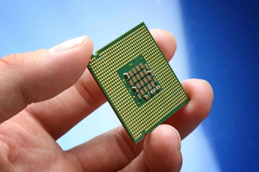
Ic package substrate manufacture. we can produce the best samllest bump pitch with 100um, the best smallest trace are 9um. and the smallest gap are 9um. most of the design are 15um to 30um trace and spacing. In the dynamic world of electronics, IC Package Substrates take center stage. These unassuming yet crucial components play a pivotal role in enabling the functionality of our everyday devices, connecting chips, and ensuring the efficient operation of a wide range of electronic products. In this comprehensive exploration, we delve deep into the heart of IC Package Substrates, uncovering their intricate construction, multifaceted applications, and the remarkable advantages they bring to the electronics industry.
Introducing IC Package Substrates
IC Package Substrates, often working behind the scenes, are the unsung heroes of modern electronics. These specialized boards provide the foundation for the assembly of semiconductor devices, fostering connections and offering a robust platform for various integrated circuits (ICs). They are, in essence, the unsung architects of the electronic world, shaping the landscape for the components that power our lives.
Emphasizing their Significance in the Electronics Industry
The electronics industry is a relentless engine of innovation and advancement. At its core lies the need for miniaturization, performance enhancement, and optimal thermal management. IC Package Substrates stand at the crossroads of these imperatives, facilitating breakthroughs in design and functionality. Without them, the electronic devices we rely on daily, from smartphones to automobiles, would be a mere aspiration.
Previewing the Discussion on the Structure, Applications, and Advantages of Package Substrates
Within this article, we will embark on a journey to demystify IC Package Substrates, unveiling their intricate structure, wide-ranging applications, and the significant advantages they offer. We will explore how these substrates are constructed, the materials that form their foundation, and the complex manufacturing processes involved. Furthermore, we will examine their practical applications, from chip packaging to circuit interconnection and thermal management.
But it doesn’t end there. We will also delve into the remarkable advantages of IC Package Substrates, highlighting their role in achieving high integration, optimizing electrical performance, and managing heat effectively. Through real-world case studies and a glimpse into the future, we will provide a comprehensive understanding of how IC Package Substrates continue to shape the landscape of the electronics industry, adapting to emerging trends and embracing new challenges. Join us on this illuminating journey through the heart of IC Package Substrates.
Structure of IC Package Substrates
Material Selection
In the intricate design of IC package substrates, the careful selection of materials plays a pivotal role.
1.Substrate Materials: These materials, often composed of robust yet lightweight compounds such as fiberglass-reinforced epoxy resin, form the base upon which the entire structure is built.
2.Conductive Layers: The inclusion of conductive layers, typically made of copper, facilitates the efficient transmission of electrical signals within the substrate.
3.Insulation Layers: To ensure the insulation of delicate circuitry, specialized insulating layers, often composed of materials like polyimide, are integrated into the substrate.
Manufacturing Process
The manufacturing process of IC package substrates involves a sequence of intricate steps, each crucial for the successful construction of the final product.
1.Substrate Material Preparation: This initial step involves the meticulous preparation of the substrate materials, including cutting, shaping, and surface treatment, to achieve the desired characteristics.
2.Layer Stacking and Lamination: Different layers, including conductive and insulating layers, are precisely stacked and laminated together to form the foundation of the substrate.
3.Drilling and Copper Plating: Subsequent drilling of precise holes and the application of copper plating onto these holes ensure the establishment of vital conductive pathways.
4.Etching and Pattern Formation: Through meticulous etching techniques, specific patterns and circuitry are formed on the substrate, defining the pathways for electrical conduction.
Surface Coating and Soldering
The final stages of the production process involve surface coating and soldering, which are essential for both protection and connectivity.
Surface Coating: Protective layers such as solder mask and surface finish are applied to shield the delicate circuitry from environmental factors and ensure long-term durability.
Soldering: With the help of soldering techniques, components are securely attached to the substrate, creating a robust and reliable connection essential for the proper functioning of the integrated circuits.
By meticulously following these material selection and manufacturing processes, IC package substrates are crafted with precision, ensuring optimal performance and reliability in a wide array of electronic applications.
Applications of IC Package Substrates
Package substrates find diverse applications in the electronics industry, each contributing to the efficient functioning of electronic devices. Here, we’ll delve into these applications, emphasizing the role of IC package substrates in various aspects of electronic engineering:
Chip Packaging
1.BGA (Ball Grid Array Packaging): BGA packaging is a prominent application of package substrates. It involves connecting the silicon chip to the substrate using an array of solder balls. This method offers high density and reliability in interconnections, making it suitable for microprocessors and other high-performance chips. The package substrate plays a vital role in ensuring these connections are stable and electrically efficient.
2.CSP (Chip Scale Packaging): CSP represents a miniaturized approach to chip packaging, reducing the overall package size by placing the semiconductor chip directly onto the package substrate. It requires precise design and manufacturing processes to ensure efficient interconnection and thermal management. Package substrates for CSP applications are engineered to provide a stable foundation for these compact chip-scale packages.
Circuit Interconnection
1.SMT (Surface Mount Technology): Surface Mount Technology is a widely used method for attaching electronic components directly to the surface of printed circuit boards (PCBs). Package substrates play a crucial role in SMT by providing a stable platform for mounting components, ensuring proper electrical connections, and offering thermal management to prevent overheating of the components. They are instrumental in achieving high-density, high-performance electronic assemblies.
2.Hard and Soft Interconnects: Package substrates facilitate both hard and soft interconnections in electronic circuits. Hard interconnects involve rigid, permanent connections such as soldered joints, while soft interconnects can include flexible printed circuits or connectors. Package substrates need to accommodate and support various interconnection methods to meet the specific needs of different electronic applications.
Thermal Management
1.Effective Heat Dissipation: Efficient thermal management is crucial for electronic devices, especially those with high-power components. Package substrates are engineered to dissipate heat effectively to prevent overheating and ensure the longevity and reliability of electronic components. Conductive layers within the substrate can act as thermal pathways, transferring heat away from sensitive components.
2.Temperature Control: Package substrates also aid in temperature control. In applications where maintaining a specific operating temperature is vital, such as in power electronics, the substrate can be designed to regulate temperature through heat sinks, thermally conductive materials, or other cooling methods. This is critical for preventing temperature-related performance issues and ensuring the longevity of electronic systems.
In summary, package substrates play a multifaceted role in chip packaging, circuit interconnection, and thermal management in the electronics industry. Their design and material choices are integral to the success of these applications, allowing for high-density, high-performance electronic systems while ensuring reliability and efficient heat management.
Advantages of Package Substrates
IC package substrates offer a myriad of advantages, making them a cornerstone in modern electronics. Let’s delve into these benefits:
High Integration
1.Compact Design: One of the primary advantages of package substrates is their ability to facilitate compact designs. By providing a robust foundation for components and interconnections, these substrates enable the creation of smaller and more efficient electronic devices. This not only results in sleek and lightweight products but also enhances portability.
2.High Performance: Package substrates play a crucial role in achieving high performance in electronic systems. Their compactness allows for shorter interconnections between components, reducing signal path lengths and minimizing latency. As a result, electronic devices equipped with package substrates exhibit faster data transfer rates and lower power consumption, ultimately enhancing overall performance.
Electrical Performance
1.Low Signal Interference: Package substrates are engineered to minimize signal interference. Their well-defined conductive paths and controlled impedance characteristics reduce crosstalk and electromagnetic interference. This, in turn, ensures that signals remain clean and reliable, contributing to the stability of electronic circuits.
2.Electromagnetic Compatibility: The inherent design of package substrates promotes electromagnetic compatibility (EMC). They are constructed to shield sensitive components from external electromagnetic noise while also preventing emissions that might interfere with other devices. As a result, products incorporating package substrates are more likely to pass EMC compliance tests and operate harmoniously within complex electronic environments.
Thermal Management
1.Efficient Heat Dissipation: Effective thermal management is paramount in the world of electronics. Package substrates are equipped with features such as thermally conductive materials and integrated heat sinks, enabling efficient heat dissipation. This is especially critical in high-performance applications, like data centers and power electronics, where excess heat can lead to reduced component lifespan and decreased reliability.
2.Temperature Control: Package substrates also aid in precise temperature control. They allow for the integration of thermal sensors and control circuits that help maintain optimal operating temperatures. This capability is crucial for preventing overheating, which can lead to component failure and system instability.
Incorporating these advantages, package substrates empower electronics designers to create innovative, reliable, and high-performance products. Whether it’s a compact, cutting-edge smartphone or a robust automotive control unit, these substrates are the unsung heroes that ensure our devices run efficiently and seamlessly, meeting the ever-evolving demands of the electronics industry.
Real-world Case Studies
Mobile Device Applications
1.Smartphones: IC package substrates play a pivotal role in the design of modern smartphones. Their compact size and high integration capabilities make them ideal for housing various electronic components, ensuring the device remains slim and efficient. This allows for advanced features such as powerful processors and high-resolution displays while maintaining portability.
2.Wearable Technology: Wearables like smartwatches and fitness trackers rely on package substrates to provide a compact yet functional design. The substrates enable the connection of various sensors and processors in a small form factor, ensuring wearers can track their health and receive notifications conveniently.
Automotive Electronics
1.Engine Control Units (ECUs): In the automotive industry, package substrates are crucial for ECUs, which are responsible for controlling various aspects of a vehicle, from engine performance to emissions. These substrates ensure the reliability and durability needed for the demanding conditions within a car’s engine bay.
2.Infotainment Systems: Package substrates are also used in infotainment systems, providing the necessary connectivity and performance for entertainment, navigation, and communication in modern vehicles. They contribute to a seamless user experience and connectivity with smartphones and other devices.
Communication Equipment
Network Switches and Routers: Package substrates are the backbone of network switches and routers, enabling high-speed data transfer and routing in data centers and communication networks. They help maintain low signal interference and high-speed data processing, essential for a reliable and efficient network infrastructure.
Satellite Communication: In the realm of satellite communication equipment, package substrates facilitate the transmission and reception of signals in the challenging environment of space. Their compact design and thermal management capabilities are essential for ensuring the smooth operation of communication satellites.
In these real-world case studies, we see how IC package substrates are integral to various industries and applications, including mobile devices, automotive electronics, and communication equipment. Their unique features and advantages enable the development of cutting-edge technology and ensure reliability in demanding environments, underscoring their importance in modern electronics.
Future Outlook
Emerging Trends in Package Substrate Technology
1.Advanced material integration for enhanced performance and durability
2.Miniaturization and increased functional density for improved efficiency
3.Integration of AI and IoT capabilities for smarter and more interconnected devices
Potential New Application Areas
1.Medical Electronics: Utilizing package substrates for advanced medical devices and diagnostic tools
2.Renewable Energy Systems: Implementing package substrates in energy-efficient systems for sustainable power generation
3.Aerospace and Defense: Leveraging package substrate technology for robust and reliable electronic components in critical aerospace and defense applications
Possible Challenges and Solutions
1.Thermal Dissipation Issues: Implementing innovative cooling solutions and heat management techniques to mitigate overheating risks
2.Cost Constraints: Exploring cost-effective materials and streamlined manufacturing processes without compromising quality and performance
3.Environmental Sustainability: Fostering the development of eco-friendly materials and recycling practices to minimize the environmental impact of package substrate production and disposal.
By addressing these emerging trends, potential new application areas, and probable challenges and solutions, the article not only highlights the current significance of IC package substrates but also offers a glimpse into their potential future, ensuring that readers are well-informed about the evolving landscape of this crucial technology.