
Low CET PCB manufacturing
Low CET PCB Manufacturing. ther are too many types Low CET PCB base materials. High TG FR4 base, BT base. ABF base, and Most high speed materials are CET base. we can use this base to produce the Low CET PCBs with high quality.
Low CET PCBs are manufactured using materials with low chlorine, bromine, and other halogen content to reduce environmental impact. The manufacturing process strictly adheres to environmental standards, selecting halogen-free or low-halogen materials and employing eco-friendly manufacturing techniques. These printed circuit boards not only comply with relevant regulations but also offer high-quality electronic performance and reliability. Low CET PCBs aim to decrease halogen emissions during the manufacturing of electronic products, promoting environmental sustainability and driving the green electronics industry forward.
What is Low CET PCB?
Low CET PCB manufacturingand package substrate manufacturing. We use advanced Msap and Sap technology, High multilayer interconnection substrates from 4 to 18 layers,
“Low CET PCB” stands for “Low Chlorine, Bromine, and other halogens Content Printed Circuit Board.” These types of PCBs are designed with materials that have reduced levels of halogen-based flame retardants, such as chlorine and bromine.
The use of halogenated flame retardants in electronics has raised environmental concerns due to their persistence in the environment and potential toxicity when released during disposal or recycling processes. Low CET PCBs are developed as a more environmentally friendly alternative, aiming to minimize the environmental impact associated with electronic waste.
Manufacturers often adhere to specific standards and regulations, such as the Restriction of Hazardous Substances (RoHS) directive, which restricts the use of certain hazardous materials, including halogens, in electrical and electronic equipment. Low CET PCBs help electronics manufacturers comply with such regulations while also reducing the environmental footprint of their products.
Low CET PCB manufacturing
What are the Low CET PCB Design Guidelines?
The Low CET PCB design guidelines mainly focus on printed circuit boards (PCBs) with low levels of chlorine, bromine, and other halogens. These guidelines aim to ensure that the design and manufacturing processes minimize or completely eliminate the use of harmful halogen substances. Here are some common Low CET PCB design guidelines:
- Material Selection: Choose environmentally friendly materials that comply with regulations, such as substrates and coating materials that are free from chlorine, bromine, and other halogens.
- Flame Retardant Selection: Opt for halogen-free or low-halogen flame retardants as alternatives to traditional chlorine- or bromine-based ones.
- Layered Board Design: When designing multilayer boards, avoid using halogen-containing laminates. Prefer materials that are free from halogens.
- Printing Techniques: Choose lead-free soldering processes and ensure that halogen-free fluxes or cleaning agents are used during the printing process.
- Reprocessability: Design PCBs for ease of recycling and reprocessing. Avoid using materials that are difficult to separate for future handling and recycling.
- Performance Evaluation: Perform performance evaluations and testing on new materials and designs to ensure they meet the standards and requirements of Low CET PCBs.
- Compliance with Regulations: Strictly adhere to relevant environmental regulations and standards, such as the RoHS directive, to ensure product compliance.
These guidelines help to minimize the use of harmful halogen substances during the design and manufacturing processes, thereby enhancing the environmental performance and sustainability of electronic products.
What is the Low CET PCB Fabrication Process?
The Low CET PCB fabrication process is similar to that of traditional PCB fabrication, with a focus on using materials and techniques that minimize or eliminate the presence of chlorine, bromine, and other halogens. Here’s an overview of the typical steps involved in the fabrication process for Low CET PCBs:
- Material Selection: Choose substrates, laminates, and solder mask materials that are free from or have low levels of halogens. This may involve selecting materials that comply with environmental regulations such as RoHS.
- Design: Create the PCB layout and design using CAD (Computer-Aided Design) software, taking into consideration the requirements for low halogen content and environmental compliance.
- Preparation: Prepare the substrate material by cutting it to the required size and cleaning it to remove any contaminants that could affect the adhesion of the copper layers.
- Copper Cladding: Apply a thin layer of copper foil to one or both sides of the substrate material using an adhesive or heat and pressure (laminating). This forms the conductive layers of the PCB.
- Etching: Use chemical etching or other methods to remove excess copper from the substrate, leaving behind the desired copper traces and patterns as per the PCB design.
- Drilling: Drill holes in the PCB at specified locations for component mounting and interconnection between layers (for multilayer PCBs).
- Plating: Plate the drilled holes with a thin layer of conductive material (typically copper) to ensure good electrical connections between layers.
- Surface Finish: Apply a surface finish to protect the exposed copper traces and pads from oxidation and provide a solderable surface. Common surface finishes for Low CET PCBs include ENIG (Electroless Nickel Immersion Gold) and HASL (Hot Air Solder Leveling).
- Solder Mask Application: Apply a solder mask over the PCB surface, leaving openings for solder pads and vias. The solder mask helps protect the copper traces and pads while also providing insulation between conductive elements.
- Silkscreen Printing: Optionally, print component designators, logos, and other information on the PCB surface using silkscreen printing.
- Testing and Inspection: Conduct electrical testing, visual inspection, and other quality control measures to ensure the PCB meets the design specifications and quality standards.
- Final Finishing: Cut the PCB panels into individual boards, clean them thoroughly, and package them for shipment or assembly.
Throughout the fabrication process, strict adherence to low halogen content guidelines and environmental regulations is essential to ensure the resulting PCBs are environmentally friendly and compliant with industry standards.
How do you manufacture a Low CET PCB?
Manufacturing a Low CET (Low Chlorine, Bromine, and other halogens Content) PCB involves specific steps and considerations aimed at reducing or eliminating the use of halogen-containing materials. Here’s a general outline of the process:
- Material Selection: Choose substrate materials, laminates, solder mask, and surface finishes that are free from or have low levels of halogens. This may involve opting for materials certified to meet environmental regulations such as RoHS (Restriction of Hazardous Substances).
- Design: Create the PCB layout and design using CAD (Computer-Aided Design) software, keeping in mind the requirements for low halogen content and environmental compliance.
- Preparation: Prepare the substrate material by cutting it to the required size and cleaning it thoroughly to remove any contaminants that could affect adhesion.
- Copper Cladding: Apply copper foil to one or both sides of the substrate material using an adhesive or lamination process. This forms the conductive layers of the PCB.
- Etching: Use chemical etching or other methods to selectively remove excess copper from the substrate, leaving behind the desired copper traces and patterns according to the PCB design.
- Drilling: Drill holes in the PCB at specified locations for component mounting and interconnection between layers (if it’s a multilayer PCB).
- Plating: Plate the drilled holes with a thin layer of conductive material (typically copper) to ensure good electrical connections between layers.
- Surface Finish: Apply a surface finish to protect the exposed copper traces and pads from oxidation and provide a solderable surface. Common surface finishes for Low CET PCBs include ENIG (Electroless Nickel Immersion Gold) and HASL (Hot Air Solder Leveling).
- Solder Mask Application: Apply a solder mask over the PCB surface, leaving openings for solder pads and vias. The solder mask helps protect the copper traces and pads while also providing insulation between conductive elements.
- Silkscreen Printing: Optionally, print component designators, logos, and other information on the PCB surface using silkscreen printing.
- Testing and Inspection: Conduct electrical testing, visual inspection, and other quality control measures to ensure the PCB meets the design specifications and quality standards.
- Final Finishing: Cut the PCB panels into individual boards, clean them thoroughly, and package them for shipment or assembly.
Throughout the manufacturing process, it’s crucial to adhere strictly to low halogen content guidelines and environmental regulations to ensure the resulting PCBs are environmentally friendly and compliant with industry standards.
How much should a Low CET PCB cost?
The cost of a Low CET PCB can vary based on several factors including the size, complexity, quantity, and specific requirements of the PCB. However, in general, Low CET PCBs may incur slightly higher costs compared to traditional PCBs due to the specialized materials and manufacturing processes involved in reducing or eliminating halogen content.
Here are some factors that can influence the cost of Low CET PCBs:
- Material Cost: Low CET materials may be more expensive than traditional materials due to their compliance with environmental regulations and specialized formulations.
- Manufacturing Processes: Certain manufacturing processes, such as using halogen-free substrates and surface finishes, may require additional steps or specialized equipment, which can contribute to higher manufacturing costs.
- Quality and Compliance: Ensuring compliance with environmental regulations and quality standards may involve additional testing and quality control measures, which can increase production costs.
- Volume: The quantity of PCBs ordered can affect the unit cost. Typically, larger volume orders may result in lower per-unit costs due to economies of scale.
- Design Complexity: PCBs with complex designs, multiple layers, or fine-pitch components may require more intricate manufacturing processes and quality control measures, which can increase costs.
- Additional Features: Optional features such as impedance control, blind/buried vias, and controlled depth drilling can add to the overall cost of the PCB.
It’s essential to obtain quotes from multiple PCB manufacturers and suppliers to get an accurate estimate of the cost for a specific Low CET PCB project. Additionally, working closely with a manufacturer to optimize the design for cost-effectiveness while meeting environmental requirements can help minimize costs without compromising quality or compliance.
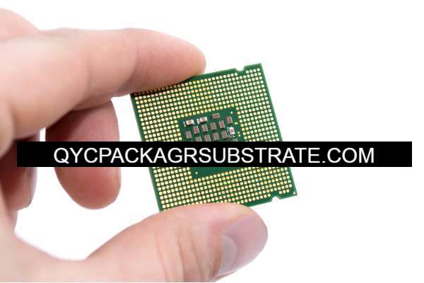
What is Low CET PCB base material?
The base material for Low CET (Low Chlorine, Bromine, and other halogens Content) PCBs refers to the substrate material used to construct the PCB. In Low CET PCBs, the base material is selected to have reduced levels of halogens, specifically chlorine, bromine, and other halogens, compared to traditional PCB base materials.
Typically, Low CET PCBs use substrate materials that are free from or have low levels of halogens to minimize environmental impact and comply with regulations such as RoHS (Restriction of Hazardous Substances). Common base materials for Low CET PCBs include:
- Halogen-free FR-4: FR-4 (Flame Retardant 4) is a widely used substrate material for PCBs due to its excellent electrical and mechanical properties. Halogen-free FR-4 variants are formulated without halogenated flame retardants, reducing the overall halogen content of the PCB.
- Polyimide (PI): Polyimide substrates are known for their high-temperature resistance and excellent dimensional stability, making them suitable for applications requiring reliability under harsh conditions. Halogen-free polyimide materials are available for Low CET PCBs.
- PTFE (Polytetrafluoroethylene): PTFE-based substrates offer low dielectric constant and loss, as well as excellent high-frequency performance. Halogen-free PTFE materials are used in specialized applications where high-frequency performance is critical.
- Other Halogen-free Materials: Besides FR-4, polyimide, and PTFE, there are various other halogen-free substrate materials available for Low CET PCBs, including BT (Bismaleimide Triazine) resin, ceramic-filled laminates, and more.
These base materials provide the foundation for the PCB’s structure, supporting the copper traces and providing insulation between conductive layers. By selecting halogen-free or low-halogen base materials, manufacturers can produce Low CET PCBs that meet environmental regulations and minimize the environmental impact of electronic products.
Which company makes Low CET PCB?
our company can also produce Low CET PCB base materials. As a specialized manufacturer of PCB materials, we are committed to developing and producing halogen-free base materials that meet environmental requirements. Our production processes and quality control systems strictly adhere to relevant environmental regulations and standards, ensuring that our produced base materials have low halogen content. We employ advanced material formulations and manufacturing techniques to offer various types of low halogen base materials, such as low halogen FR-4, polyimide (PI), PTFE, etc., to meet customers’ demands for Low CET PCBs.
With an experienced technical team and advanced production equipment, our company can flexibly address custom requirements from customers while ensuring the quality and performance of the products. Through collaboration with us, customers can obtain high-quality, environmentally friendly Low CET PCB base materials, providing a reliable foundation for their electronic products.
What are the 7 qualities of good customer service?
Good customer service is characterized by several key qualities that contribute to positive interactions and relationships between businesses and their customers. Here are seven qualities of good customer service:
- Responsiveness: Good customer service involves being prompt and responsive to customer inquiries, requests, and concerns. Responding to customers in a timely manner shows that you value their time and are committed to addressing their needs promptly.
- Empathy: Empathy is the ability to understand and empathize with the customer’s perspective, feelings, and situation. Good customer service representatives listen actively, show genuine concern for the customer’s issue, and strive to put themselves in the customer’s shoes to provide personalized assistance.
- Clear Communication: Effective communication is essential for good customer service. Clear, concise, and respectful communication helps ensure that customers understand the information provided and feel confident in the support they receive. Avoiding jargon and using language that is easy for customers to understand is key.
- Problem-Solving Skills: Good customer service involves being proactive and resourceful in resolving customer issues and addressing their concerns. Customer service representatives should possess strong problem-solving skills, be able to think critically, and offer creative solutions to meet customers’ needs.
- Professionalism: Professionalism encompasses various aspects of behavior and demeanor, including courtesy, respect, and integrity. Good customer service representatives maintain a professional attitude at all times, regardless of the situation, and strive to build trust and credibility with customers.
- Adaptability: Customers have diverse needs and preferences, so good customer service involves being adaptable and flexible in accommodating different customer requirements. Customer service representatives should be able to adapt their approach and communication style to suit the individual needs of each customer.
- Follow-Up: Following up with customers after resolving their issues or completing a transaction demonstrates commitment to customer satisfaction and helps maintain positive relationships. Good customer service involves following up to ensure that the customer’s needs were met satisfactorily and addressing any remaining concerns or feedback.
By embodying these qualities, businesses can provide exceptional customer service experiences that foster customer loyalty, satisfaction, and long-term success.
FAQs
What are the benefits of using Low CET PCBs?
Low CET PCBs offer improved thermal stability, which enhances the reliability and performance of electronic devices, particularly in applications with demanding thermal environments.
Can Low CET PCBs be used in high-temperature applications?
Yes, Low CET PCBs are suitable for high-temperature environments where traditional PCBs may experience thermal expansion-related issues, leading to performance degradation or failure.
Are Low CET PCBs more expensive than standard PCBs?
Generally, yes, Low CET PCBs may have a slightly higher cost due to the specialized materials and manufacturing processes involved. However, the benefits in terms of reliability and performance often justify the investment.
What industries benefit most from Low CET PCBs?
Industries such as aerospace, automotive, telecommunications, and industrial electronics, which require high reliability and performance in challenging thermal environments, can benefit significantly from the use of Low CET PCBs.