
Microvia Package Substrate Manufacturer
We are a professional Microvia Package Substrate Manufacturer, we mainly produce ultra-small bump pitch substrate, ultra-small trace and spacing packaging substrate and PCBs.
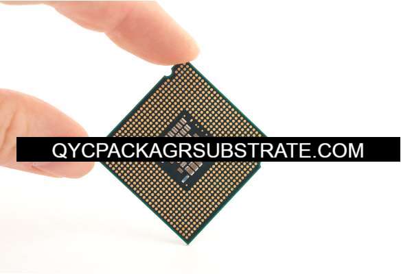
Microvia Package Substrate is a pivotal component in modern electronic packaging, revolutionizing the way electronic devices are designed and manufactured. This advanced substrate technology enables the creation of compact, high-performance electronic devices by providing a platform for intricate interconnects and signal routing. By utilizing microvias—tiny holes drilled into the substrate—Microvia Package Substrates offer unparalleled routing density and signal integrity, making them ideal for applications where space is at a premium and high-speed performance is essential.
These substrates are fabricated through a meticulous process involving precision drilling, copper plating, pattern imaging, and surface finishing, resulting in a substrate that meets stringent performance and reliability requirements. With their ability to support miniaturization, improved thermal management, and enhanced electrical performance, Microvia Package Substrates are driving innovation across industries, from consumer electronics to telecommunications and automotive applications. In essence, they represent the backbone of modern electronic systems, enabling the development of smaller, faster, and more efficient devices to meet the demands of today’s interconnected world.
What is a Microvia Package Substrate?
A Microvia Package Substrate is a crucial component in electronic packaging, especially in the manufacturing of semiconductor devices like integrated circuits (ICs) and microprocessors. It serves as a platform for connecting various components within the package, facilitating the transmission of electrical signals between them.
At its core, a Microvia Package Substrate consists of a thin layer of insulating material, typically made of epoxy resin or a similar substrate material. Embedded within this insulating layer are tiny holes called microvias, hence the name. These microvias are typically less than 100 micrometers in diameter, allowing for extremely dense routing of electrical connections.
The primary function of these microvias is to establish electrical connections between different layers of the substrate and the components mounted on its surface. This enables the transmission of signals between the integrated circuits, passive components, and other elements of the electronic system.
Microvia Package Substrates offer several advantages over traditional packaging methods:
- Miniaturization: Microvias enable the design of smaller and more compact electronic devices, making them ideal for applications where space is limited, such as smartphones, wearables, and IoT devices.
- Improved Signal Integrity: The shorter signal paths provided by microvias help minimize signal loss and electromagnetic interference, resulting in improved signal integrity and overall performance of the electronic system.
- High Density Interconnects: Microvias allow for the creation of high-density interconnects, enabling the integration of more components and functionality into a single package.
- Enhanced Thermal Management: Microvia Package Substrates can be designed with features such as thermal vias and copper traces to improve heat dissipation and thermal management, ensuring the reliability and longevity of the electronic device.
- Increased Bandwidth: The high-density routing capabilities of microvias enable the transmission of high-speed signals with greater bandwidth, making them suitable for applications requiring high data transfer rates, such as data centers and high-performance computing.
Overall, Microvia Package Substrates play a critical role in advancing the capabilities of modern electronic devices by enabling smaller form factors, improved performance, and enhanced functionality. As technology continues to evolve, the demand for more advanced and efficient packaging solutions like Microvia Package Substrates is expected to grow.
Microvia Package Substrate Manufacturer
What are the Microvia Package Substrate Design Guidelines?
Microvia Package Substrate design guidelines are essential principles and best practices that engineers follow to ensure the optimal performance, reliability, and manufacturability of electronic packages utilizing microvia technology. Here are some key design guidelines:
- Microvia Aspect Ratio: Maintain a balanced aspect ratio (the ratio of hole diameter to board thickness) to ensure proper plating and reliability. A typical aspect ratio range is 0.8 to 1.2.
- Microvia Size and Pitch: Determine the appropriate microvia size and pitch based on the density of the interconnects required for the application. Smaller microvias allow for higher routing densities but may increase manufacturing complexity.
- Minimum Annular Ring: Ensure an adequate annular ring (the copper pad around the microvia) to provide sufficient electrical connectivity and mechanical support. Typically, the annular ring width should be at least equal to the microvia diameter.
- Layer Staggering: Stagger microvias between adjacent layers to minimize signal crosstalk and improve routing efficiency. Proper staggering can also enhance thermal performance and reduce manufacturing issues such as registration errors.
- Signal Integrity Considerations: Follow signal integrity principles such as controlled impedance routing, differential pair routing, and minimizing signal reflections to maintain signal integrity and minimize electromagnetic interference (EMI).
- Thermal Management:Incorporate thermal vias and heat dissipation features into the substrate design to manage thermal issues effectively. Proper thermal management helps prevent overheating and ensures the reliability of the electronic components.
- Dielectric Material Selection: Choose dielectric materials with appropriate electrical, mechanical, and thermal properties to meet the specific requirements of the application. Consider factors such as dielectric constant, thermal conductivity, and coefficient of thermal expansion (CTE).
- Design for Manufacturability (DFM): Optimize the substrate design for manufacturability by considering factors such as panel utilization, material utilization, and ease of manufacturing processes such as drilling, plating, and etching.
- Alignment and Registration: Ensure precise alignment and registration of microvias and other features during manufacturing to avoid misalignment issues that can impact electrical performance and reliability.
- Reliability Testing: Perform reliability testing, such as thermal cycling, mechanical shock, and vibration testing, to validate the robustness of the substrate design and ensure long-term reliability in real-world operating conditions.
By adhering to these Microvia Package Substrate design guidelines, engineers can develop electronic packages that meet the stringent requirements of modern electronic devices in terms of performance, reliability, and manufacturability.
What is the Microvia Package Substrate Fabrication Process?
The fabrication process of Microvia Package Substrates involves several steps to create the intricate interconnects and insulating layers required for electronic packaging. Here’s a general overview of the fabrication process:
- Substrate Preparation: The process begins with preparing a substrate material, typically a laminate composed of layers of epoxy resin and glass fiber. The substrate material is cleaned and inspected to ensure it meets the required specifications.
- Drilling Microvias: Small-diameter holes, known as microvias, are drilled into the substrate material using laser drilling or mechanical drilling techniques. Laser drilling is often preferred for its precision and ability to create very small diameter holes.
- Cleaning and Desmearing: After drilling, the substrate is cleaned to remove any debris or contaminants generated during the drilling process. A desmear process may also be performed to remove resin smear from the walls of the microvias, ensuring proper plating adhesion.
- Copper Plating:A thin layer of copper is deposited onto the walls of the microvias and onto the surface of the substrate through an electroplating process. This copper plating forms the conductive pathways for electrical interconnects.
- Pattern Imaging: A photoresist material is applied to the substrate surface, and a photolithography process is used to selectively expose and develop the photoresist, creating a pattern that defines the circuit traces and component pads.
- Etching:The exposed copper areas not protected by the photoresist are etched away using chemical etchants, leaving behind the desired copper traces and pads on the substrate surface.
- Surface Finishing:Surface finishing processes such as immersion gold, electroless nickel immersion gold (ENIG), or organic solderability preservative (OSP) may be applied to the exposed copper surfaces to improve solderability and protect against oxidation.
- Solder Mask Application: A solder mask is applied to the substrate surface to cover the copper traces and pads, leaving only the areas where solder connections are required exposed. The solder mask helps prevent solder bridges and protects the copper features from environmental damage.
- Final Inspection and Testing: The fabricated Microvia Package Substrates undergo thorough inspection and testing to ensure they meet the required specifications for dimensional accuracy, electrical connectivity, and reliability. This may include visual inspection, electrical testing, and mechanical testing.
- Assembly: Once fabricated, the Microvia Package Substrates are ready for component assembly. Integrated circuits, passive components, and other electronic elements are mounted onto the substrate using soldering techniques such as surface mount technology (SMT) or flip-chip bonding.
By following this fabrication process with precision and care, manufacturers can produce Microvia Package Substrates that meet the demanding requirements of modern electronic devices in terms of miniaturization, performance, and reliability.
How do you manufacture a Microvia Package Substrate?
Manufacturing a Microvia Package Substrate involves a series of intricate processes aimed at creating a precise and reliable platform for electronic components. Here’s a step-by-step guide to the manufacturing process:
- Substrate Material Selection: Choose a substrate material suitable for the specific application, typically a laminate composed of epoxy resin and glass fiber. The substrate material should have the necessary mechanical, thermal, and electrical properties.
- Preparation and Cleaning: Clean the substrate material to remove any contaminants or impurities that could affect the manufacturing process or the performance of the final product. This may involve processes such as washing, rinsing, and drying.
- Laser Drilling: Use laser drilling technology to create microvias, which are small-diameter holes, in the substrate material. Laser drilling offers high precision and the ability to create very small features, making it ideal for microvia fabrication.
- Copper Plating: Coat the walls of the microvias and the surface of the substrate with a thin layer of copper through an electroplating process. This copper plating establishes the conductive pathways for electrical interconnects.
- Etching and Imaging: Apply a photoresist material to the substrate surface and use photolithography techniques to selectively expose and develop the photoresist, creating a pattern that defines the circuit traces and component pads. Etch away the exposed copper areas using chemical etchants, leaving behind the desired copper features.
- Surface Finishing: Apply surface finishes such as immersion gold, electroless nickel immersion gold (ENIG), or organic solderability preservative (OSP) to the exposed copper surfaces. These surface finishes improve solderability and protect against oxidation.
- Solder Mask Application:Apply a solder mask to the substrate surface to cover the copper traces and pads, leaving only the areas where solder connections are required exposed. The solder mask helps prevent solder bridges and protects the copper features from environmental damage.
- Final Inspection and Testing: Inspect the fabricated Microvia Package Substrates for dimensional accuracy, electrical connectivity, and reliability. This may involve visual inspection, electrical testing, and mechanical testing to ensure the substrates meet the required specifications.
- Assembly: Once fabricated and inspected, the Microvia Package Substrates are ready for component assembly. Electronic components such as integrated circuits, passive components, and connectors are mounted onto the substrate using soldering techniques such as surface mount technology (SMT) or flip-chip bonding.
- Packaging and Shipping: Package the assembled substrates appropriately to protect them during transportation and storage. Ensure proper labeling and documentation before shipping the substrates to customers or assembly facilities for integration into electronic devices.
By following these manufacturing steps with precision and attention to detail, manufacturers can produce high-quality Microvia Package Substrates that meet the demanding requirements of modern electronic devices.
How much should a Microvia Package Substrate cost?
The cost of a Microvia Package Substrate can vary widely depending on several factors, including the substrate material, size, complexity of the design, number of layers, technology used (such as laser drilling), surface finishes, and quantity ordered.
Here are some key factors that can influence the cost:
- Substrate Material: Different substrate materials have different costs. High-performance materials with specialized properties may be more expensive than standard materials.
- Size and Complexity: Larger substrates with more complex designs and higher layer counts generally cost more to manufacture due to increased material and processing requirements.
- Technology Used: Advanced technologies such as laser drilling for microvias or specialized surface finishes can increase manufacturing costs.
- Surface Finishes: The choice of surface finish can impact the cost. Premium finishes like immersion gold may cost more than standard finishes like HASL (Hot Air Solder Leveling).
- Quantity: Economies of scale typically apply, meaning that larger production runs can lower the per-unit cost due to spreading fixed costs over more units.
- Lead Time: Rush orders or expedited manufacturing may incur additional fees.
It’s challenging to provide a specific cost without knowing the exact specifications of the Microvia Package Substrate needed. However, as a rough estimate, Microvia Package Substrates can range from a few dollars to several tens of dollars per square inch, with more complex or high-performance substrates costing more.
To get an accurate cost estimate, it’s best to consult with a manufacturer or supplier and provide detailed specifications for the desired substrate, including dimensions, material requirements, layer count, technology preferences, and expected quantity. They can then provide a customized quote based on your specific needs and volume requirements.
What is Microvia Package Substrate base material?
The base material used for Microvia Package Substrates typically consists of laminates made from epoxy resin and glass fiber. These laminates are commonly referred to as FR-4 (Flame Retardant 4) or similar materials. FR-4 is a widely used substrate material in the electronics industry due to its excellent electrical insulation properties, mechanical strength, and affordability.
FR-4 is composed of layers of woven glass fiber impregnated with an epoxy resin binder. This combination results in a robust and durable substrate material that can withstand the thermal and mechanical stresses encountered during the manufacturing process and in the final application.
In addition to FR-4, other substrate materials may be used depending on the specific requirements of the application. For example, high-frequency applications may require substrates with low dielectric constant and loss tangent, such as polytetrafluoroethylene (PTFE) or ceramic-filled materials. High-temperature applications may necessitate substrates with enhanced thermal stability, such as polyimide-based materials.
Ultimately, the choice of base material for Microvia Package Substrates depends on factors such as electrical performance, thermal management requirements, cost considerations, and the specific needs of the end application.
Which company makes Microvia Package Substrates?
There are many companies with rich experience and expertise in manufacturing Microvia Package Substrates. Some well-known companies include Hitachi Chemical, Toray, Kyocera in Japan, Micron Technology, Intel, Foxconn in the United States, and Compal Electronics, Unimicron in Taiwan.
Our company also has the capability to produce Microvia Package Substrates. As a company specializing in electronics manufacturing, we have advanced manufacturing equipment, extensive experience, and a high-quality team. Our engineering team has deep technical backgrounds and expertise to design and manufacture high-quality Microvia Package Substrates according to customer requirements.
In our manufacturing facility, we employ advanced processes and quality control measures to ensure that each Microvia Package Substrate meets strict specifications and standards. We use certified high-quality materials to guarantee the reliability and stability of our products.
Our company offers various customization options, including different substrate materials, layer counts, microvia sizes, surface treatments, and size requirements, to meet the diverse application needs of our customers. Whether in the fields of communication, computing, medical, automotive, or industrial control, we can provide the most suitable Microvia Package Substrate solutions.
Additionally, we prioritize customer service and communication, aiming to establish long-term cooperative relationships with our customers. We are committed to listening to customer needs and feedback, providing timely technical support and solutions. We will continue to strive for continuous improvement in technology and manufacturing capabilities to deliver better products and services to our customers.
What are the 7 qualities of good customer service?
Good customer service is characterized by several key qualities that contribute to a positive experience for customers. Here are seven qualities:
- Responsiveness: Good customer service involves promptly addressing customer inquiries, concerns, and requests. This includes responding to emails, phone calls, and messages in a timely manner and being available to assist customers when needed.
- Empathy: Empathy is the ability to understand and relate to the feelings and perspectives of customers. Good customer service representatives demonstrate empathy by actively listening to customers, acknowledging their concerns, and showing genuine care and concern for their needs.
- Professionalism: Professionalism entails maintaining a courteous, respectful, and knowledgeable demeanor when interacting with customers. This includes communicating clearly and effectively, adhering to company policies and procedures, and representing the company in a positive light.
- Problem-solving skills: Good customer service representatives possess strong problem-solving skills to effectively address customer issues and resolve conflicts. They are proactive in finding solutions, taking ownership of problems, and following through until the issue is resolved to the customer’s satisfaction.
- Flexibility:Flexibility is essential in adapting to the diverse needs and preferences of customers. Good customer service involves being adaptable and accommodating, whether it’s adjusting to changes in customer requests, accommodating special requests, or finding creative solutions to unique problems.
- Reliability: Reliability is the consistency and dependability of the service provided to customers. Good customer service entails delivering on promises, meeting or exceeding customer expectations, and consistently providing high-quality assistance and support.
- Positive attitude: Maintaining a positive attitude is crucial in creating a welcoming and enjoyable customer service experience. Good customer service representatives approach interactions with optimism, enthusiasm, and a willingness to help, creating a positive atmosphere that fosters trust and loyalty.
By embodying these qualities, businesses can cultivate strong relationships with their customers, foster loyalty, and differentiate themselves in a competitive market.
FAQs
What is a Microvia Package Substrate?
A Microvia Package Substrate is a critical component in electronic packaging, providing a platform for connecting various components within a semiconductor device. It typically consists of a thin layer of insulating material with small holes called microvias for routing electrical connections.
What are the advantages of using Microvia Package Substrates?
Microvia Package Substrates offer advantages such as miniaturization, improved signal integrity, high-density interconnects, enhanced thermal management, and increased bandwidth. These benefits contribute to the development of smaller, more efficient electronic devices.
How are Microvia Package Substrates fabricated?
The fabrication process involves steps such as drilling microvias, copper plating, pattern imaging, etching, surface finishing, solder mask application, and final inspection. These processes create the intricate interconnects and insulating layers required for electronic packaging.
What base materials are used for Microvia Package Substrates?
Microvia Package Substrates are typically made from laminates composed of epoxy resin and glass fiber, commonly known as FR-4. Other materials such as polyimide-based materials or ceramic-filled materials may be used for specific applications.
What factors influence the cost of Microvia Package Substrates?
The cost of Microvia Package Substrates varies depending on factors such as substrate material, size, complexity of design, technology used, surface finishes, and quantity ordered. Larger production runs and standard materials may lower costs, while advanced technologies and customizations may increase costs.
What companies manufacture Microvia Package Substrates?
Several companies specialize in the manufacturing of Microvia Package Substrates, including Hitachi Chemical, Toray, Kyocera, Micron Technology, Intel, Foxconn, Compal Electronics, and Unimicron, among others.
What are the key design guidelines for Microvia Package Substrates?
Design guidelines include considerations such as microvia aspect ratio, size, and pitch, minimum annular ring, layer staggering, signal integrity, thermal management, dielectric material selection, design for manufacturability, alignment and registration, and reliability testing.