
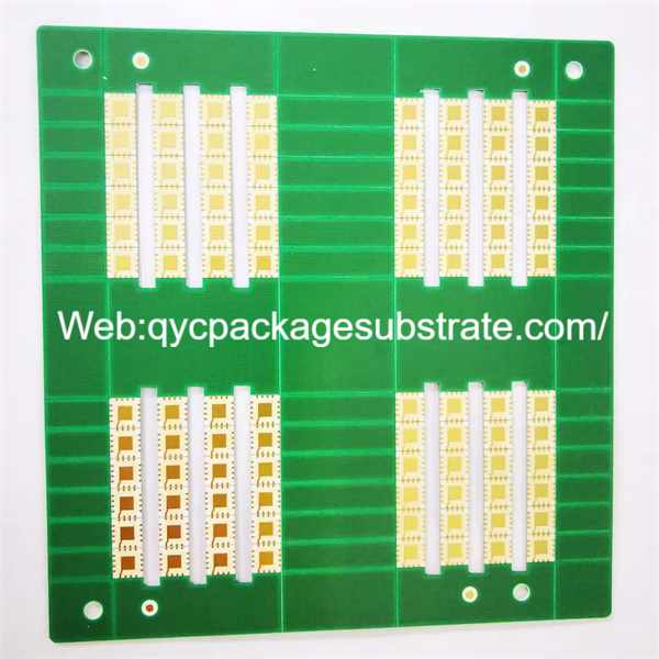
Microvias PCB manufacturing
Microvias PCB manufacturing, HDI PCB made with Microvias. the best smallest laser via holes size are 2mil. we have made the HDI Microvias PCB from 4 layer to 30 layers. Microvias PCBs revolutionize the landscape of printed circuit board technology, offering unparalleled advantages in compactness, signal integrity, and high-frequency performance. These boards feature small-diameter plated through-holes, known as microvias, which serve as the conduit for interconnecting different layers within the PCB. By utilizing advanced drilling and plating techniques, Microvias PCBs enable designers to achieve higher routing densities and more intricate layouts, making them ideal for applications requiring miniaturization and high-density interconnects.
With their ability to facilitate shorter signal paths and minimize signal distortion, Microvias PCBs are essential in high-frequency applications such as telecommunications, wireless communication systems, and radar systems. Furthermore, their compact size and lightweight construction make them well-suited for portable electronic devices where space constraints are paramount.
Manufacturing Microvias PCBs demands precision and expertise, ensuring the integrity and reliability of the final product. As technology continues to evolve, Microvias PCBs remain at the forefront of innovation, driving advancements in electronics and empowering the development of next-generation devices.
What is a Microvias PCB?
Microvias PCB manufacturing and package substrate manufacturing. We use advanced Msap and Sap technology, High multilayer interconnection substrates from 4 to 18 layers,
A Microvias PCB (Printed Circuit Board) refers to a type of PCB that utilizes microvias, which are tiny holes drilled into the board for routing connections between different layers of the PCB. These microvias are typically smaller in diameter than traditional vias, allowing for denser routing and more compact circuit designs.
Microvias are especially useful in high-density interconnect (HDI) PCBs, where space is limited and signal integrity is crucial. They enable designers to pack more components and routing traces into a smaller area, making them suitable for applications like smartphones, tablets, wearable devices, and other compact electronics.
There are different types of microvias, including stacked microvias and filled microvias. Stacked microvias involve multiple layers of vias stacked on top of each other, allowing for even greater routing density. Filled microvias are filled with conductive or non-conductive materials to enhance reliability and improve signal integrity.
Overall, Microvias PCBs are essential for achieving high-performance and miniaturization in modern electronic devices.
Microvias PCB manufacturing
What are Microvias PCB Design Guidelines?
Microvias are small diameter plated through-holes used in printed circuit boards (PCBs) to connect adjacent layers of the board. They are commonly employed in high-density interconnect (HDI) PCB designs to facilitate the routing of fine-pitch components and signal traces.
Here are some general guidelines for designing PCBs with microvias:
- Minimum Size and Aspect Ratio: The size and aspect ratio (the ratio of hole depth to diameter) of microvias should be carefully chosen based on the manufacturing capabilities of your PCB fabrication house. Generally, microvias have diameters ranging from 75 to 150 microns, and aspect ratios up to 1:1 are common.
- Pad Size and Annular Ring: Ensure that the pad size and annular ring (the copper area around the hole) are sufficient to provide good electrical and mechanical connection. The pad size should be large enough to accommodate the microvia and provide a reliable solder joint.
- Keepout Zones: Maintain adequate keepout zones around microvias to prevent interference with adjacent components, traces, or other features on the PCB. This helps to avoid electrical or mechanical conflicts during assembly and operation.
- Placement and Routing: Carefully plan the placement and routing of microvias to optimize signal integrity and minimize signal distortion. Microvias should be strategically located to reduce signal path lengths and impedance mismatches.
- Via Stubs: Minimize the length of via stubs (the portion of the via that extends beyond the adjacent layer) to reduce signal reflections and improve signal integrity. This can be achieved by using blind or buried microvias where applicable.
- Thermal Considerations: Consider the thermal implications of microvia placement and routing, especially in high-power or high-temperature applications. Avoid placing microvias near heat-generating components or in areas of high thermal stress.
- Manufacturing Constraints: Consult with your PCB fabrication house early in the design process to ensure that your microvia design is compatible with their manufacturing capabilities and processes. Consider factors such as minimum drill sizes, aspect ratio limitations, and preferred materials.
- Signal Integrity Analysis: Perform signal integrity analysis, such as impedance calculations and crosstalk simulations, to validate the performance of microvias in your design. This helps to ensure that signal quality meets the requirements of your application.
By following these guidelines and considering the specific requirements of your PCB design, you can effectively incorporate microvias to achieve high-density interconnects and optimal signal integrity in your circuit board layouts.
What is the Microvias PCB Fabrication Process?
The fabrication process for PCBs with microvias involves several steps, including design, material selection, drilling, plating, imaging, etching, and finishing. Here’s an overview of the microvias PCB fabrication process:
- Design: The design phase involves creating the PCB layout using computer-aided design (CAD) software. During this stage, the designer specifies the location, size, and configuration of microvias based on the requirements of the circuit and the desired density of interconnections.
- Material Selection: Choose the appropriate laminate material for the PCB based on factors such as dielectric constant, thermal properties, and mechanical strength. High-performance materials like FR-4, polyimide, or specialty materials optimized for microvia fabrication may be used.
- Drilling: Microvias are typically drilled using laser drilling or mechanical drilling techniques. Laser drilling offers precise control over hole size and placement, while mechanical drilling is more cost-effective for larger holes. Laser drilling is preferred for microvias due to its ability to create smaller diameter holes with higher precision.
- Desmear and Cleaning: After drilling, the holes are cleaned and desmeared to remove any debris or residues generated during the drilling process. Desmearing is essential to ensure good adhesion of the plating to the walls of the microvias.
- Electroless Copper Deposition:A thin layer of electroless copper is deposited onto the walls of the microvias to provide a conductive surface for subsequent plating steps. This step is crucial for ensuring good electrical connectivity between the layers of the PCB.
- Electroplating: Electroplating is used to build up the thickness of the copper layer inside the microvias and on the surface of the PCB. The plated copper provides the conductive pathways for electrical signals and connections between layers.
- Imaging and Etching: A photoresist layer is applied to the surface of the PCB, and a photolithography process is used to transfer the PCB design onto the photoresist. The exposed areas of the photoresist are then etched away, leaving behind the copper traces and pads.
- Final Finishing: After etching, the PCB may undergo additional processes such as surface finish application (e.g., solder mask, HASL, ENIG) and legend printing. These finishing steps provide protection and labeling for the PCB, as well as facilitate soldering and assembly.
- Inspection and Testing:The finished PCBs are inspected for defects and undergo electrical testing to ensure that they meet the specified performance criteria. This may include continuity testing, impedance testing, and other quality checks.
- Routing and Profiling: The individual PCBs are routed out of the larger panel and profiled to their final dimensions using mechanical or laser cutting techniques.
By following these steps, PCB manufacturers can produce high-quality circuit boards with microvias that meet the requirements of various high-density and high-performance applications.
How do you manufacture a Microvias PCB?
Manufacturing a PCB with microvias involves several intricate steps. Here’s a detailed overview of the microvias PCB fabrication process:
- Design: The PCB design is created using CAD software, specifying the layout, dimensions, and location of microvias according to the circuit requirements.
- Material Selection: Choose the appropriate laminate material based on the application requirements and performance criteria. High-performance materials such as FR-4, polyimide, or specialty materials optimized for microvia fabrication are commonly used.
- Drilling: Microvias are typically drilled using either laser drilling or mechanical drilling techniques. Laser drilling offers precise control over hole size and placement, making it suitable for creating small-diameter microvias. Mechanical drilling is more cost-effective for larger holes.
- Desmear and Cleaning: After drilling, the PCB is cleaned and desmeared to remove any debris or residues generated during the drilling process. Desmearing is essential to ensure good adhesion of the plating to the walls of the microvias.
- Electroless Copper Deposition: A thin layer of electroless copper is deposited onto the walls of the microvias to provide a conductive surface for subsequent plating steps. This step is crucial for ensuring good electrical connectivity between the layers of the PCB.
- Electroplating: Electroplating is used to build up the thickness of the copper layer inside the microvias and on the surface of the PCB. The plated copper provides the conductive pathways for electrical signals and connections between layers.
- Imaging and Etching: A photoresist layer is applied to the surface of the PCB, and the PCB design is transferred onto the photoresist using photolithography. The exposed areas of the photoresist are then etched away, leaving behind the copper traces and pads, including those within the microvias.
- Final Finishing: After etching, the PCB may undergo additional processes such as surface finish application (e.g., solder mask, HASL, ENIG) and legend printing. These finishing steps provide protection and labeling for the PCB, as well as facilitate soldering and assembly.
- Inspection and Testing: The finished PCBs are inspected for defects and undergo electrical testing to ensure that they meet the specified performance criteria. This may include continuity testing, impedance testing, and other quality checks.
- Routing and Profiling: The individual PCBs are routed out of the larger panel and profiled to their final dimensions using mechanical or laser cutting techniques.
By following these steps with precision and attention to detail, PCB manufacturers can produce high-quality circuit boards with microvias that meet the requirements of various high-density and high-performance applications.
How much should a Microvias PCB cost?
The cost of a microvias PCB can vary significantly depending on various factors such as board size, complexity, number of layers, material selection, surface finish, and quantity. However, due to the added complexity and specialized manufacturing processes involved in producing microvias, they tend to be more expensive compared to traditional PCBs without microvias.
As a rough estimate, you can expect the cost of a microvias PCB to be anywhere from 2 to 10 times more expensive than a standard PCB without microvias. This cost increase is primarily due to the additional steps involved in drilling, plating, and processing microvias, as well as the higher precision required in manufacturing.
For a more accurate cost estimate, it’s best to consult with PCB manufacturers or suppliers directly, providing them with detailed specifications of your PCB design and requirements. They can provide you with a quote based on your specific needs and volume of production.
Additionally, factors such as economies of scale, negotiation with suppliers, and choice of materials and surface finishes can also influence the final cost of microvias PCBs. Therefore, it’s essential to consider these factors and optimize your design and manufacturing process to minimize costs while meeting your performance requirements.
What is Microvias PCB base material?
The base material for microvias PCBs can vary depending on the specific requirements of the application and the manufacturing process used. However, some commonly used materials for microvias PCBs include:
- FR-4: FR-4 (Flame Retardant 4) is a widely used epoxy-based laminate material that offers good electrical insulation properties and mechanical strength. It is cost-effective and suitable for many applications, including those requiring microvias.
- High-Frequency Laminates: High-frequency laminates, such as Rogers RO4000 series or Taconic TLY series, are specially engineered for applications requiring excellent electrical performance at high frequencies. These materials typically have low dielectric loss, consistent electrical properties, and good thermal stability, making them suitable for microvias PCBs in RF and microwave applications.
- Polyimide:Polyimide materials, such as DuPont’s Pyralux, are flexible and offer excellent thermal and chemical resistance. They are often used in flexible PCBs or applications where flexibility is required, and they can also be used in microvias PCBs.
- BT Epoxy: Bismaleimide Triazine (BT) epoxy materials provide high thermal stability and are suitable for high-temperature applications. They offer good electrical properties and are commonly used in microvias PCBs for applications where thermal performance is critical.
- Specialty Materials: There are also specialty materials available that are specifically designed for microvias PCBs, offering features such as enhanced thermal conductivity, low dielectric loss, or controlled coefficient of thermal expansion (CTE) to meet the requirements of specific applications.
When selecting the base material for a microvias PCB, it’s essential to consider factors such as electrical performance, thermal properties, mechanical strength, cost, and manufacturability. Working closely with your PCB manufacturer or supplier can help ensure that the chosen material meets your performance requirements while being compatible with the microvias fabrication process.
Which company makes Microvias PCB?
There are many companies that can produce Microvias PCBs, some well-known ones include PCB manufacturers such as Foxconn, Pusongda, and JLCPCB, as well as suppliers specialized in high-performance PCBs such as Rogers, Isola, and others.
Our company can also manufacture Microvias PCBs, whether they are single-sided, double-sided, or multi-layered PCBs, we can customize production according to customer requirements. We have advanced manufacturing equipment and technology to meet various Microvias PCB manufacturing requirements. Our manufacturing process includes high-precision drilling, copper plating, imaging, etching, and other steps to ensure the quality and precision of Microvias.
Our manufacturing capabilities are not limited to traditional blind vias and buried vias, but also include Mixed Microvias. Mixed Microvias PCB combines blind vias, buried vias, and regular vias, enabling higher board density and more complex layout designs. This technology is particularly suitable for applications requiring higher performance and more compact designs, such as high-speed data transmission, wireless communication, medical devices, and other fields.
Our engineering team has rich experience and professional knowledge, able to provide customized design recommendations and solutions to meet specific technical and performance requirements of customers. We are committed to providing customers with high-quality, reliable Microvias PCB products, ensuring timely delivery and excellent after-sales service.
Whatever type of Microvias PCB your project requires, we can customize production according to your specifications and requirements. Feel free to contact us, let’s collaborate to provide high-quality PCB solutions for your project.
What are the 7 qualities of good customer service?
Good customer service is essential for building and maintaining strong relationships with customers. Here are seven qualities that characterize good customer service:
- Responsiveness: Good customer service involves promptly addressing customer inquiries, concerns, and requests. Responding to customers in a timely manner demonstrates attentiveness and a commitment to meeting their needs promptly.
- Empathy: Empathy involves understanding and acknowledging the customer’s feelings, concerns, and perspectives. Empathetic customer service representatives listen actively, show genuine concern, and strive to understand the customer’s situation to provide appropriate assistance and support.
- Clarity: Effective communication is essential for providing good customer service. Customer service representatives should convey information clearly and concisely, avoiding jargon or technical language that may confuse or alienate customers. Clear communication helps ensure that customers understand the assistance provided and the steps to resolve their issues.
- Professionalism: Professionalism encompasses maintaining a positive attitude, remaining courteous and respectful, and conducting oneself with integrity and honesty. Customer service representatives should strive to uphold high standards of professionalism in all interactions with customers, regardless of the circumstances.
- Problem-solving Skills: Good customer service involves effectively resolving customer issues and complaints. Customer service representatives should possess strong problem-solving skills, including the ability to identify root causes, explore possible solutions, and implement appropriate actions to address customer concerns and achieve satisfactory outcomes.
- Flexibility: Flexibility is essential for adapting to the diverse needs and preferences of customers. Customer service representatives should be adaptable and willing to accommodate customer requests, preferences, and special circumstances whenever possible. Flexibility helps enhance customer satisfaction and loyalty by demonstrating a willingness to go the extra mile to meet their needs.
- Follow-up: Following up with customers after resolving their issues or inquiries is an important aspect of good customer service. Following up shows that the company values the customer’s feedback and is committed to ensuring their satisfaction. It also provides an opportunity to address any additional concerns or questions the customer may have and further strengthen the relationship.
By embodying these qualities, businesses can deliver exceptional customer service experiences that foster trust, loyalty, and positive word-of-mouth recommendations from satisfied customers.
FAQs (Frequently Asked Questions)
What are Microvias PCBs?
Microvias PCBs are printed circuit boards that feature small diameter plated through-holes, known as microvias, which connect different layers of the board. These microvias enable high-density interconnects and are commonly used in applications requiring compact layouts and high-frequency signals.
What are the advantages of using Microvias PCBs?
Some advantages of Microvias PCBs include increased routing density, reduced signal distortion, improved signal integrity, and enhanced thermal performance. They also allow for smaller PCB footprints, lighter weight, and potentially lower costs compared to traditional through-hole vias.
How are Microvias PCBs manufactured?
The manufacturing process for Microvias PCBs involves drilling small-diameter holes (microvias) using laser or mechanical drilling techniques, followed by plating, imaging, etching, and finishing processes. These steps create the necessary interconnections between layers while maintaining high precision and reliability.
What are the different types of Microvias?
Microvias can be classified into different types based on their structure and functionality. Common types include blind microvias, which connect an outer layer to one or more inner layers, and buried microvias, which connect inner layers without penetrating the outer layers. Mixed Microvias combine blind, buried, and through-hole vias for increased design flexibility.
What factors should be considered when designing Microvias PCBs?
When designing Microvias PCBs, factors such as signal integrity, thermal management, manufacturability, material selection, and cost should be carefully considered. It’s important to optimize the layout and placement of microvias to ensure reliable electrical performance and efficient heat dissipation.
What applications are suitable for Microvias PCBs?
Microvias PCBs are commonly used in high-frequency applications such as telecommunications, wireless communication systems, RF/microwave circuits, radar systems, and high-speed data transmission. They are also utilized in compact electronic devices where space constraints and signal integrity are critical.
How can I ensure the reliability of Microvias PCBs?
Ensuring the reliability of Microvias PCBs involves using high-quality materials, following best practices in design and manufacturing, conducting thorough testing and quality control measures, and working with reputable PCB manufacturers with expertise in Microvias fabrication. Additionally, adhering to industry standards and guidelines can help maintain reliability standards.