
Minimum Clearance Circuit Board Manufacturer
Minimum Clearance Circuit Board Manufacturer,Minimum Clearance Circuit Boards are designed with precise spacing to ensure reliable operation in compact electronic devices. These boards are engineered to meet strict design rules that minimize the distance between conductive traces, pads, and other features while maintaining electrical isolation and preventing signal interference. This careful attention to clearance is crucial for high-density applications where space is limited, such as in mobile devices, wearables, and advanced electronics. By adhering to minimum clearance standards, these circuit boards support enhanced performance, reduce the risk of short circuits, and enable the integration of more components within a smaller footprint, ensuring efficient and reliable functionality.
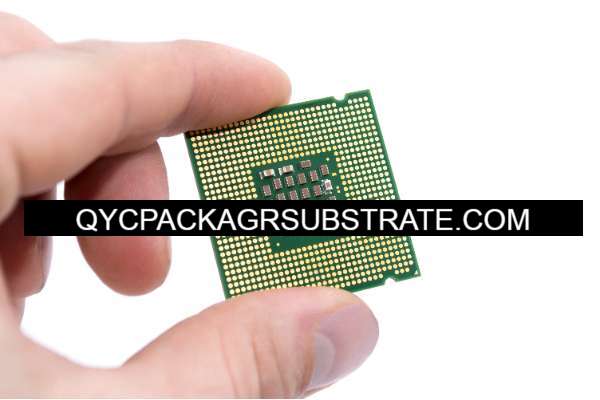
What is a Minimum Clearance Circuit Board (MCCB)?
A Minimum Clearance Circuit Board (MCCB) is a specialized type of printed circuit board (PCB) engineered with exceptionally tight tolerances and minimal spacing between conductive elements. The term “minimum clearance” pertains to the smallest distance allowed between traces, pads, and other components on the PCB. This design approach is particularly crucial for applications where space is limited and high-density circuit layouts are required.
MCCBs are commonly used in compact, high-performance electronic devices such as advanced consumer electronics, medical devices, telecommunications equipment, and aerospace systems. The tight spacing allows for a higher density of components and connections, optimizing the use of board space and potentially enhancing the overall performance and functionality of the device.
Achieving the tight clearances required for MCCBs demands advanced fabrication technologies and precise manufacturing techniques. This includes high-resolution photolithography, accurate etching processes, and meticulous quality control measures. Such precision is necessary to avoid issues like electrical shorts, signal interference, and heat dissipation problems that can arise from closely spaced conductive elements.
Additionally, MCCBs must comply with industry standards and safety regulations, which govern the minimum required clearances to prevent electrical faults and ensure reliable operation. These standards help mitigate risks associated with reduced spacing, such as increased potential for short circuits and reduced insulation effectiveness.
In summary, Minimum Clearance Circuit Boards are designed to fit more functionality into a smaller footprint, leveraging advanced manufacturing techniques and stringent standards to achieve high-density layouts while maintaining reliability and performance.
Minimum Clearance Circuit Board Manufacturer
What are the MCCB Design Guidelines?
Designing a Minimum Clearance Circuit Board (MCCB) involves several critical guidelines to ensure functionality, reliability, and manufacturability. Here are the key design guidelines for MCCBs:
- Clearance Specifications: Adhere to strict clearance requirements between traces, pads, and other conductive elements. These clearances must meet industry standards and be defined based on the voltage levels and signal integrity needs of the application. Ensuring proper spacing is crucial to prevent electrical shorts and ensure reliable operation.
- Trace Width and Spacing: Design traces with appropriate widths to handle the required current without excessive heat generation. For tight clearances, precise trace width and spacing calculations are essential to maintain signal integrity and prevent overheating. Use software tools to simulate and verify trace dimensions and spacing.
- Signal Integrity: Consider signal integrity issues such as crosstalk and impedance matching. With minimal clearance, closely spaced traces can lead to signal interference. Employ techniques such as differential signaling, controlled impedance traces, and proper routing practices to mitigate these issues.
- Thermal Management: Minimize thermal problems by incorporating adequate heat dissipation strategies. In high-density designs, thermal vias, heat sinks, and efficient component placement help manage heat generated by closely packed components.
- Manufacturing Tolerances: Work closely with PCB manufacturers to understand their capabilities and limitations regarding minimal clearances. Ensure that the design files are optimized for the fabrication process and that any special requirements are communicated clearly.
- Design for Testability: Include test points and design features that facilitate testing and troubleshooting. This is especially important in high-density boards where visibility and access to components may be limited.
- Component Placement: Optimize component placement to reduce trace lengths and minimize interference. Proper arrangement helps manage electrical performance and thermal issues, particularly in high-density designs.
- Compliance with Standards: Ensure the design complies with relevant industry standards and regulations. This includes standards for electrical clearance, safety, and manufacturability.
- Review and Verification:Conduct thorough design reviews and simulations to verify that the MCCB meets all performance and reliability criteria. Use Design Rule Checks (DRC) and Electrical Rule Checks (ERC) to catch potential issues before fabrication.
- 10. Prototype Testing:Fabricate prototypes and perform extensive testing to validate the design. This helps identify and address any issues related to the tight clearances and overall functionality before full-scale production.
In summary, designing a Minimum Clearance Circuit Board requires careful attention to clearance specifications, signal integrity, thermal management, and compliance with manufacturing and safety standards. Following these guidelines helps ensure that the high-density board performs reliably and meets the required technical and safety criteria.
What is the MCCB Fabrication Process?
The fabrication process for a Minimum Clearance Circuit Board (MCCB) involves several precise and controlled steps to ensure that the board meets stringent design specifications and performance requirements. Here’s a detailed overview of the MCCB fabrication process:
- Design and Layout: The process begins with the creation of detailed circuit designs using Electronic Design Automation (EDA) tools. The design includes all aspects such as trace routing, component placement, and clearance specifications. The design files are reviewed and optimized to ensure they meet the tight clearance requirements and adhere to industry standards.
- Photomask Preparation: Once the design is finalized, photomasks are prepared. These masks are used to transfer the circuit pattern onto the PCB substrate. The photomasks are created based on the design files and must be highly accurate to achieve the minimal clearances specified.
- Substrate Preparation: The PCB substrate, typically a laminate material like FR4 or a high-frequency material, is prepared. For MCCBs, high-quality substrates with precise thickness and minimal defects are crucial. The substrate is cleaned and treated to ensure proper adhesion of subsequent layers.
- Copper Clad Laminate: A copper foil is laminated onto the substrate to create a copper-clad laminate. The thickness of the copper layer is chosen based on current-carrying requirements and design specifications. The laminate is then inspected for uniformity and defects.
- Pattern Transfer: The circuit pattern is transferred onto the copper-clad laminate using photolithography. A photosensitive resist is applied to the copper surface, and the photomask is used to expose the resist to ultraviolet light. This process creates a pattern on the resist that corresponds to the desired circuit layout.
- Etching: After pattern transfer, the exposed copper is etched away using chemical solutions, leaving behind only the desired circuit traces and pads. The etching process must be precisely controlled to maintain the minimal clearances and avoid damage to the fine traces.
- Drilling and Via Formation: Holes are drilled into the PCB to create vias and component mounting holes. For MCCBs, precision drilling is essential to ensure accurate alignment and minimal spacing. The vias are typically plated to create electrical connections between different layers of the board.
- Layer Stacking and Lamination: If the MCCB design includes multiple layers, the individual layers are stacked and laminated together. This involves aligning the layers, applying adhesive, and subjecting the stack to heat and pressure to bond the layers into a single, cohesive board.
- Surface Finish: A surface finish is applied to protect the exposed copper and ensure good solderability. Common finishes include HASL (Hot Air Solder Leveling), ENIG (Electroless Nickel Immersion Gold), or OSP (Organic Solderability Preservative).
- Inspection and Testing: The fabricated MCCB undergoes rigorous inspection and testing. This includes visual inspections, automated optical inspections (AOI), and electrical testing to verify that the board meets the design specifications and functions correctly.
- Routing and Depanelization: The individual MCCBs are separated from the larger panel using routing or depanelization techniques. This step ensures that the final boards are cut to the correct size and shape while maintaining the integrity of the tight clearances.
- Final Quality Control: The final boards are subjected to a final quality control check, including electrical testing, mechanical inspection, and dimensional verification. Any defects or deviations from the design are addressed before the boards are shipped to customers.
In summary, the fabrication of a Minimum Clearance Circuit Board involves precise design, advanced photolithography, careful etching, and rigorous testing. Each step is critical to ensuring that the board meets the stringent requirements for minimal clearance and high-density design.
How Do You Manufacture a Minimum Clearance Circuit Board?
Manufacturing a Minimum Clearance Circuit Board (MCCB) involves several precise and detailed processes to ensure the board meets design specifications and performance standards. Here’s a step-by-step overview:
- Design and Layout: Begin with detailed PCB design and layout using specialized software. Ensure that all minimum clearance requirements are adhered to, and optimize trace routing, component placement, and thermal management.
- Material Selection: Choose appropriate PCB materials based on the design requirements, including the type of dielectric material and copper thickness. The materials should support the desired electrical and thermal performance.
- Photographic Imaging: Transfer the PCB design onto a photo-sensitive laminate using a photographic imaging process. This involves applying a photoresist layer to the copper-clad laminate and exposing it to UV light through the design mask.
- Etching: After exposure, develop the photoresist to reveal the copper pattern. The board is then subjected to an etching process, usually involving a chemical solution that removes unwanted copper, leaving only the desired circuit traces.
- Drilling: Drill holes for through-hole components and vias. Precision drilling machines are used to create these holes according to the design specifications, ensuring minimal clearance between drilled holes and traces.
- Plating: Apply a layer of metal (usually copper) to the interior surfaces of drilled holes through an electroplating process. This creates conductive pathways between different layers of the PCB.
- Solder Mask Application: Apply a solder mask layer to protect the copper traces from oxidation and prevent solder from bridging between traces during component soldering. This layer must be precisely aligned with the circuit traces.
- Silkscreen Printing: Print identifying marks, component labels, and other information on the board’s surface using a silkscreen process. This layer aids in assembly and component placement.
- Final Etching and Cleaning:Perform a final etching to remove any residual copper and clean the board to eliminate contaminants and residues from previous processes.
- Inspection and Testing: Conduct thorough inspection and testing to verify the board’s quality and functionality. Automated Optical Inspection (AOI) and electrical testing are commonly used to detect defects and ensure compliance with design specifications.
- Assembly: Once the board is validated, proceed with component placement and soldering. This may involve manual or automated assembly processes, depending on the complexity and volume of production.
- Final Inspection:Perform a final inspection of the assembled PCB to ensure all components are correctly placed and soldered, and that the board meets all performance and reliability standards.
By meticulously following these steps, manufacturers can produce high-quality MCCBs that meet the stringent requirements of modern electronic devices.
How Much Should a Minimum Clearance Circuit Board Cost?
The cost of a Minimum Clearance Circuit Board (MCCB) can vary significantly based on several factors, including design complexity, manufacturing processes, materials, and volume. Here’s a breakdown of the factors that influence the cost:
- Design Complexity: More complex designs with high-density components and minimal clearances typically cost more due to the increased precision required in manufacturing and inspection.
- Layer Count: MCCBs can be single-sided, double-sided, or multi-layered. Multi-layer boards are more expensive due to the additional processes involved, such as layer bonding and inner-layer plating.
- Material Specifications: High-quality or specialized materials, such as high-frequency laminates or advanced dielectric materials, can increase the cost. Standard FR-4 materials are generally less expensive.
- Drilling and Plating: The cost of drilling fine holes and plating vias adds to the overall price. MCCBs with very small hole sizes or high aspect ratios require more advanced equipment and processes, raising the cost.
- Solder Mask and Surface Finish:Advanced solder masks and surface finishes (like ENIG or HASL) can affect the cost. Specialized finishes for better solderability or durability tend to be more expensive.
- Production Volume: The cost per unit generally decreases with higher production volumes due to economies of scale. Small batch or prototype production tends to be more expensive per board.
- Testing and Quality Assurance: Comprehensive testing, such as automated optical inspection (AOI) and electrical testing, adds to the cost. MCCBs requiring rigorous testing procedures will be priced higher.
- Lead Time:Faster turnaround times can increase costs. Standard lead times are typically more cost-effective than expedited production schedules.
These estimates are rough and can vary based on specific requirements and regional factors. For an accurate quote, it’s best to contact PCB manufacturers with detailed design specifications and production needs.
What is MCCB Base Material?
MCCB (Minimum Clearance Circuit Board) base material refers to the primary substrate or foundational layer of the PCB on which the conductive traces and components are mounted. The choice of base material is crucial as it affects the board’s electrical performance, thermal properties, and mechanical strength. Here’s a detailed look at common base materials used for MCCBs:
- FR-4: This is the most common base material for PCBs. It consists of a woven glass fabric impregnated with epoxy resin. FR-4 offers good mechanical properties, electrical insulation, and is relatively cost-effective. It is suitable for many general-purpose applications.
- CEM-1 and CEM-3: These are composite materials used in cheaper, less demanding applications. CEM-1 consists of paper-based phenolic resin, while CEM-3 is a glass-epoxy laminate similar to FR-4 but generally less durable.
- Polyimide: Polyimide is used for high-performance applications requiring excellent thermal stability and flexibility. It can withstand higher temperatures and is often used in flexible and rigid-flex PCBs.
- High-Frequency Laminates: For applications involving high-frequency signals, such as RF and microwave circuits, specialized materials like Rogers or Nelco laminates are used. These materials have low dielectric constants and losses, improving signal integrity.
- Aluminum: For applications requiring enhanced heat dissipation, aluminum-based PCBs (also known as metal-core PCBs) are used. The aluminum base helps to dissipate heat more effectively than traditional FR-4.
- Ceramic: Ceramic substrates are used in high-power and high-frequency applications. They offer superior thermal conductivity and stability, making them suitable for high-performance and high-reliability environments.
- PTFE (Teflon): PTFE is used for its low dielectric loss and high frequency stability. It is often employed in high-frequency applications where minimal signal attenuation is critical.
- Beryllium Oxide (BeO): This material is known for its excellent thermal conductivity and electrical insulation properties. It is used in high-power and high-temperature applications but is less common due to its cost and handling precautions.
Choosing the right base material for an MCCB depends on the specific requirements of the application, such as operating frequency, thermal management needs, and cost constraints.
Which Company Makes Minimum Clearance Circuit Boards?
Many companies manufacture Minimum Clearance Circuit Boards (MCCBs), including some well-known ones:
- TSMC: Although primarily known for semiconductor manufacturing, TSMC also offers high-performance PCB design and manufacturing services, with extensive experience in high-frequency and high-density applications.
- MediaTek: As a leading semiconductor company, MediaTek not only designs integrated circuits but also engages in the development and manufacturing of high-density circuit boards.
- Sunlord Electronics: This company focuses on electronic components and PCB manufacturing, including circuit boards for high-density applications.
- Renesas Electronics: They provide comprehensive PCB solutions, including Minimum Clearance Circuit Boards, serving industries such as automotive, industrial, and consumer electronics.
- Foxconn: As one of the world’s largest electronic manufacturing service providers, Foxconn has advanced PCB production capabilities and can produce various high-density and complex design circuit boards.
Our company is also capable of producing Minimum Clearance Circuit Boards (MCCBs). We have the following advantages:
- Advanced Manufacturing Equipment: We have state-of-the-art production equipment, including high-precision photolithography machines, automated drilling equipment, and precise coating technologies, ensuring high quality and reliability in the MCCBs we produce.
- High-Density Design Capability: We specialize in designing and manufacturing high-density and high-performance circuit boards, handling complex circuit layouts and minimal clearance requirements to meet customer needs in high-frequency, high-speed, and compact designs.
- Strict Quality Control: We implement rigorous quality control procedures, including Automated Optical Inspection (AOI) and electrical testing, to ensure every circuit board meets high-quality standards.
- Flexible Production Capacity: Whether for small-batch prototypes or large-scale production, we offer flexible manufacturing capabilities, quickly responding to customer needs and providing customized solutions for different application scenarios.
- Excellent Customer Service: We are committed to maintaining close communication with customers, providing technical support and professional advice to ensure each project is completed smoothly and meets expectations.
We look forward to collaborating with you to develop and manufacture high-performance Minimum Clearance Circuit Boards, helping you achieve innovative designs and outstanding performance.
What are the 7 Qualities of Good Customer Service?
Good customer service is essential for building strong relationships with clients and ensuring their satisfaction. Here are seven key qualities of excellent customer service:
- Responsiveness: Timely and efficient responses to customer inquiries, issues, and feedback are crucial. Being prompt helps to address customer concerns quickly and shows that their time and issues are valued.
- Empathy: Understanding and acknowledging the customer’s feelings and perspectives is important. Empathetic service involves actively listening to customers, validating their concerns, and demonstrating genuine care for their needs.
- Knowledgeability: Having a deep understanding of the products, services, and policies allows customer service representatives to provide accurate information and effective solutions. This expertise helps in addressing queries effectively and guiding customers appropriately.
- Patience: Patience is vital, especially when dealing with frustrated or confused customers. Maintaining a calm and composed demeanor, regardless of the situation, helps in resolving issues more effectively and ensures a positive customer experience.
- Communication Skills: Clear, concise, and courteous communication is essential. Effective customer service involves articulating information in an understandable manner, listening actively, and ensuring that all customer interactions are respectful and professional.
- Problem-Solving Abilities: The ability to quickly and effectively address and resolve customer issues is a key quality. Good customer service involves finding practical solutions to problems and ensuring that customers are satisfied with the resolution.
- Follow-Up: Ensuring that issues are fully resolved and following up with customers to confirm their satisfaction demonstrates commitment to their experience. Follow-up shows that the company values ongoing customer relationships and is dedicated to continuous improvement.
These qualities help create a positive customer experience, build trust, and encourage customer loyalty.
FAQs
What is a Minimum Clearance Circuit Board (MCCB)?
MCCBs are printed circuit boards designed with minimal spacing between conductive traces and components. This design allows for more compact and efficient layouts, suitable for high-density and high-performance applications.
Why are minimum clearances important in MCCBs?
Minimum clearances ensure electrical insulation between traces and components to prevent short circuits, signal interference, and reliability issues, especially in high-density and high-frequency applications.
What materials are used for MCCBs?
Common materials include FR-4 (a glass-epoxy laminate), high-frequency laminates (like Rogers), polyimide, and ceramic. The choice depends on factors such as electrical performance, thermal management, and cost.
How do I determine the minimum clearance requirements?
Clearance requirements are typically specified by industry standards (e.g., IPC standards) and depend on factors such as operating voltage, frequency, and environmental conditions. Consult these standards or a PCB manufacturer for specific guidelines.
What are the challenges in manufacturing MCCBs?
Challenges include maintaining precise spacing during manufacturing, managing heat dissipation, ensuring signal integrity, and meeting stringent quality control standards.
Can MCCBs be used in all types of electronic devices?
MCCBs are ideal for high-density and high-performance devices where space is limited, such as smartphones, medical devices, and advanced computing systems. However, they may not be necessary for less complex or lower-density applications.
How do I choose a PCB manufacturer for MCCBs?
Look for manufacturers with experience in high-density and high-precision PCB manufacturing, advanced equipment, and a track record of quality and reliability. Request samples and check references to ensure they can meet your specific needs.